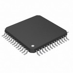
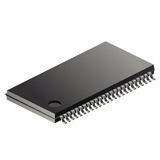
CDC582PAH
3.3 -V锁相环时钟差分LVPECL时钟输入驱动器 3.3-V PHASE-LOCK LOOP CLOCK DRIVER WITH DIFFERENTIAL LVPECL CLOCK INPUTS
The CDC582 is a high-performance, low-skew, low-jitter clock driver. It uses a phase-lock loop PLL to precisely align the frequency and phase of the clock output signals to the differential LVPECL clock CLKIN, input signals. It is specifically designed to operate at speeds from 50 MHz to 100 MHz or down to 25 MHz on outputs configured as half-frequency outputs. The CDC582 operates at 3.3-V VCC.
The feedback input FBIN synchronizes the frequency of the output clocks with the input clock CLKIN, signals. One of the twelve output clocks must be fed back to FBIN for the PLL to maintain synchronization between the differential CLKIN and inputs and the outputs. The output used as feedback is synchronized to the same frequency as the clock CLKIN and inputs.
The Y outputs can be configured to switch in phase and at the same frequency as differential clock inputs CLKIN and . Select SEL1, SEL0 inputs configure up to nine Y outputs, in banks of three, to operate at one-half or double the differential clock input frequency, depending upon the feedback configuration see Tables 1 and 2. All output signal duty cycles are adjusted to 50% independent of the duty cycle at the input clocks.
Output-enable is provided for output control. When is high, the outputs are in the low state. When is low, the outputs are active. is negative-edge triggered and can be used to reset the outputs operating at half frequency. TEST is used for factory testing of the device and can be used to bypass the PLL. TEST should be strapped to GND for normal operation.
Unlike many products containing a PLL, the CDC582 does not require external RC networks. The loop filter for the PLL is included on chip, minimizing component count, board space, and cost.
Because it is based on PLL circuitry, the CDC582 requires a stabilization time to achieve phase lock of the feedback signal to the reference signal. This stabilization time is required following power up and application of a fixed-frequency, fixed-phase signal at CLKIN and CLKIN\, as well as following any changes to the PLL reference or feedback signal. Such changes occur upon change of SEL1 and SEL0, enabling the PLL via TEST, and upon enable of all outputs via .
The CDC582 is characterized for operation from 0°C to 70°C.