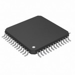
CDC536DB
具有三态输出的3.3V锁相环时钟驱动器 3.3-V PHASE-LOCK LOOP CLOCK DRIVER WITH 3-STATE OUTPUTS
The CDC536 is a high-performance, low-skew, low-jitter clock driver. It uses a phase-lock loop PLL to precisely align, in both frequency and phase, the clock output signals to the clock input CLKIN signal. It is specifically designed for use with synchronous DRAMs and popular microprocessors operating at speeds from 50 MHz to 100 MHz or down to 25 MHz on outputs configured as half-frequency outputs. The CDC536 operates at 3.3-V VCC and is designed to drive a 50-W transmission line.
The feedback input FBIN is used to synchronize the output clocks in frequency and phase to the input clock CLKIN. One of the six output clocks must be fed back to FBIN for the PLL to maintain synchronization between CLKIN and the outputs. The output used as the feedback pin is synchronized to the same frequency as CLKIN.
The Y outputs can be configured to switch in phase and at the same frequency as CLKIN. The select SEL input configures three Y outputs to operate at one-half or double the CLKIN frequency depending on which pin is fed back to FBIN see Tables 1 and 2. All output signal duty cycles are adjusted to 50% independent of the duty cycle at the input clock.
Output-enable OE\ is provided for output control. When OE\ is high, the outputs are in the high-impedance state. When OE\ is low, the outputs are active. TEST is used for factory testing of the device and can be use to bypass the PLL. TEST should be strapped to GND for normal operation.
Unlike many products containing PLLs, the CDC536 does not require external RC networks. The loop filter for the PLL is included on-chip, minimizing component count, board space, and cost.
Because it is based on PLL circuitry, the CDC536 requires a stabilization time to achieve phase lock of the feedback signal to the reference signal. This stabilization time is required following power up and application of a fixed-frequency, fixed-phase signal at CLKIN as well as following any changes to the PLL reference or feedback signals. Such changes occur upon change of the select inputs, enabling the PLL via TEST, and upon enable of all outputs via OE\\\\.
The CDC536 is characterized for operation from 0°C to 70°C.