FDG315N
FAIRCHILD SEMICONDUCTOR FDG315N 晶体管, MOSFET, N沟道, 2 A, 30 V, 120 mohm, 10 V, 1.8 V
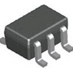
最大源漏极电压Vds Drain-Source Voltage| 30V \---|--- 最大栅源极电压Vgs± Gate-Source Voltage| 20V 最大漏极电流Id Drain Current| 2A 源漏极导通电阻ΩRds DΩ/Ohmain-SouΩ/Ohmce On-State Ω/Ohmesistance| 160mΩ@ VGS = 4.5V, ID =1.7A 开启电压Vgs(th) Gate-Source Threshold Voltage| 1~3V 耗散功率Pd Power Dissipation| 750mW/0.75W Description & Applications| N-Channel Logic Level Power Trench MOSFET General Description This N-Channel MOSFET is produced using Semiconductor"s advanced Power Trench process that has been especially tailored to minimize the on-state resistance and yet maintain low gate charge for superior switching performance. These devices are well suited for portable electronics applications. Applications • Load switch • Power management • DC/DC converter Features • Low gate charge. • High performance trench technology for extremely low RDSON. • Compact industry standard SC70-6 surface mount package. 描述与应用| N沟道逻辑电平功率沟槽MOSFET 概述 此N沟道MOSFET采用飞兆半导体先进的功率沟槽进程,已特别是针对减少通态电阻,同时保持出色的开关性能低栅极电荷。这些器件非常适合用于便携式电子产品应用。 应用 •负荷开关 •电源管理 •DC/ DC转换器 特点 •低栅极电荷。 •高性能沟道技术极低的RDS(ON)。 •紧凑型工业标准SC70-6表面贴装封装。