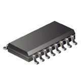
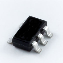
SN65LVDS19DRFT
具有使能端的 2.5V/3.3V 振荡器增益级/缓冲器 8-WSON -40 to 85
These four devices are high frequency oscillator gain stages supporting both LVPECL or LVDS on the high gain outputs in 3.3-V or 2.5-V systems. Additionally, provides the option of both single-ended input PECL levels on the SN65LVx18 and fully differential inputs on the SN65LVx19.
The SN65LVx18 provides the user a Gain Control GC for controlling the Q output from 300 mV to 860 mV either by leaving it open NC, grounded, or tied to VCC. When left open, the Q output defaults to 575 mV. The Q on the SN65LVx19 defaults to 575 mV as well.
Both devices provide a voltage reference VBB of typically 1.35 V below VCC for use in receiving single-ended PECL input signals. When not used, VBB should be unconnected or open.
All devices are characterized for operation from -40°C to 85°C.

