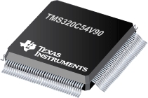
TMS320C54V90
DSP(仅限于 DSP),用于嵌入式 V90 调制解调器解决方案 [不推荐在新型设计中采用 NRND]
The is used to implement a full-featured, high-performance modem technology, intended for use in embedded systems and similar applications. This highly integrated solution implements a complete modem using only two chips: the TMS320C54V90 DSP with on-chip RAM and ROM, and the Si3016 line-side DAA.
The modem can connect to a host system serially RS-232 functionality, or as an 8-bit peripheral to the processor in a host system. The TMS320C54V90 uses a standard Digital Signal Processor DSP and proprietary firmware to perform all the modem signal processing, the V.42/V.42bis compression, and AT commands interpretation for modem control functions.
The TMS320C54V90 also uses the latest silicon DAA technology. This technology does not require a transformer and results in lower cost, lower power, and a smaller area for the DAA function.
For serial interface applications, an integrated UART implements the serial interface with no additional hardware.
- .
- Provides Two-Chip Modem Solution
- .
- Data Rates from 300 bps to 56 Kbps
- .
- Data Modulation Standards
V.90, V.34, V.32bis, V.32, V.22bis, V.22, V.23,
V.21 and V.23 reversible Minitel, Bell 212, Bell 103
- .
- FAX Capabilities
- .
- ITU-T V.17, V.29, V.27ter Modulations
- .
- A/EIA 578 Class 1 Interface
* V.42 or MNP Class 3 and 4 Error Control and V.42bis Compression
* Caller ID
* Field-Proven Modem Algorithms Give Highest Performance, Reliability, and Compatibility
* Non-Volatile EEPROM Configuration Storage
* Worldwide Telecom Approvals
* Parallel Phone Support Including Parallel Phone Detection
* Parallel Phone Exclusion Relay Control
* Protected Against Surge and Overvoltage on the Telephone Line
* Parallel Host Port Interface Supports a Variety of Industry Standard Busses
* Integral Serial Interface UART
* Autobaud on Serial DTE Interface
* State-of-the-Art Integrated Transformerless Silicon DAA for Phone Line Interconnection
* Applications
- .
- Embedded Systems
- .
- Set-Top Boxes
- .
- Gaming Consoles
- .
- Internet Appliances
- .
- Portable Devices PDAs, digital cameras
- .
- Remote Data Collection, Point-of-Sale
- .
- Meter Reading, Utility Monitoring
* 40K x 16-Bit Dual-Access On-Chip RAM
* 128K x 16-Bit On-Chip ROM
* On-Chip Peripherals
- .
- Software-Programmable Wait-State Generator and Programmable Bank Switching
- .
- On-Chip Phase-Locked Loop PLL Clock Generator With Internal Oscillator or External Clock Source
- .
- Two Multichannel Buffered Serial Ports McBSPs
- .
- Enhanced 8-Bit Parallel Host-Port Interface HPI8
* Power Consumption Control With IDLE1, IDLE2, and IDLE3 Instructions With Power-Down Modes
* On-Chip Scan-Based Emulation Logic, IEEE Std 1149.1 JTAG Boundary Scan Logic
* 8.5-ns Single-Cycle Fixed-Point Instruction Execution Time 117.96 MIPS or 17-ns Instruction Execution Time 58.98 MIPS for 3.3-V Power Supply 1.5-V Core
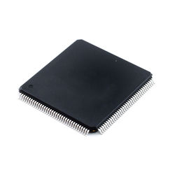
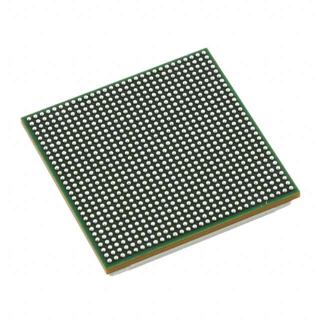
* Available in a 144-Pin Plastic Low-Profile Quad Flatpack LQFP PGE Suffix and a 144-Pin Ball Grid Array BGA GGU Suffix
**Note:** Human Body Model ESD test performance for this product was demonstrated to be ±1.5 kV during product qualification. Industry standard test method used was IEA/JESD22-A114. Adherence to ESD handling precautionary procedures is advised at all times.
All trademarks are the property of their respective owners.
IEEE Standard 1149.1-1990 Standard-Test-Access Port and Boundary Scan Architecture.