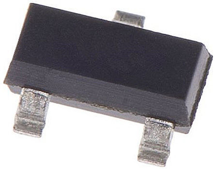
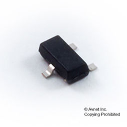
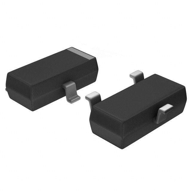
FDV302P
FAIRCHILD SEMICONDUCTOR FDV302P 晶体管, MOSFET, P沟道, -120 mA, -25 V, 7.9 ohm, -4.5 V, -1 V
最大源漏极电压VdsDrain-Source Voltage| -25V \---|--- 最大栅源极电压Vgs±Gate-Source Voltage| -8V 最大漏极电流IdDrain Current| -0.12A 源漏极导通电阻RdsDrain-Source On-State Resistance| 0.079Ω @-200mA,-4.5V 开启电压Vgs(th)Gate-Source Threshold Voltage| -0.65--1.5V 耗散功率PdPower Dissipation| 350mW/0.35W Description & Applications| Very low level gate drive requirements allowing direct operation in 3V circuits. VGSth < 1.5V. Gate-Source Zener for ESD ruggedness. >6kV Human Body Model Compact industry standard SOT-23 surface mount package. Replace many PNP digital transistors DTCx and DCDx with one DMOS FET. 描述与应用| 非常低的水平栅极驱动要求可直接 操作在3V电路。 VGS(TH)<1.5V。 门源齐纳ESD坚固。 >6kV人体模型 紧凑型工业标准SOT-23表面贴装封装。 更换众多PNP数字的(DTCx和DCDx) 具有一DMOS FET