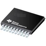
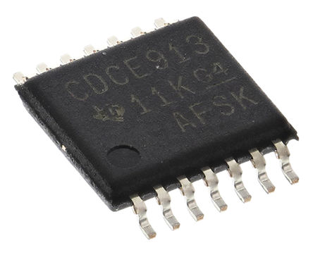
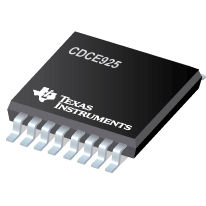
CDCE906PW
可编程3 -PLL时钟合成器/乘法器/除法器 PROGRAMMABLE 3-PLL CLOCK SYNTHESIZER / MULTIPLIER / DIVIDER
The CDCE906 is one of the smallest and powerful PLL synthesizer / multiplier / divider available today. Despite its small physical outlines, the CDCE906 is flexible. It has the capability to produce an almost independent output frequency from a given input frequency.
The input frequency can be derived from a LVCMOS, differential input clock, or a single crystal. The appropriate input waveform can be selected via the SMBus data interface controller.
To achieve an independent output frequency the reference divider M and the feedback divider N for each PLL can be set to values from 1 up to 511 for the M-Divider and from 1 up to 4095 for the N-Divider. The PLL-VCO voltage controlled oscillator frequency than is routed to the free programmable output switching matrix to any of the six outputs. The switching matrix includes an additional 7-bit post-divider 1-to-127 and an inverting logic for each output.
The deep M/N divider ratio allows the generation of zero ppm clocks from any reference input frequency e.g., a 27 MHz.
The CDCE906 includes three PLLs of those one supports SSC spread-spectrum clocking. PLL1, PLL2, and PLL3 are designed for frequencies up to 167 MHz and optimized for zero-ppm applications with wide divider factors.
PLL2 also supports center-spread and down-spread spectrum clocking SSC. This is a common technique to reduce electro-magnetic interference. Also, the slew-rate controllable SRC output edges minimize EMI noise.
Based on the PLL frequency and the divider settings, the internal loop filter components will be automatically adjusted to achieve high stability and optimized jitter transfer characteristic of the PLL.
The device supports non-volatile EEPROM programming for easy-customized application. It is preprogrammed with a factory default configuration see Figure 13 and can be reprogrammed to a different application configuration before it goes onto the PCB or reprogrammed by in-system programming. A different device setting is programmed via the serial SMBus interface.
Two free programmable inputs, S0 and S1, can be used to control for each application the most demanding logic control settings outputs disable to low, outputs 3-state, power down, PLL bypass, etc.
The CDCE906 has three power supply pins, VCC, VCCOUT1 and VCCOUT2. VCC is the power supply for the device. It operates from a single 3.3-V supply voltage. VCCOUT1 and VCCOUT2 are the power supply pins for the outputs. VCCOUT1 supplies the outputs Y0 and Y1 and VCCOUT2 supplies the outputs Y2, Y3, Y4, and Y5. Both outputs supplies can be 2.3 V to 3.6 V. At output voltages lower than 3.3 V, the output drive current is limited.
The CDCE906 is characterized for operation from 0°C to 70°C.

