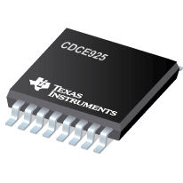
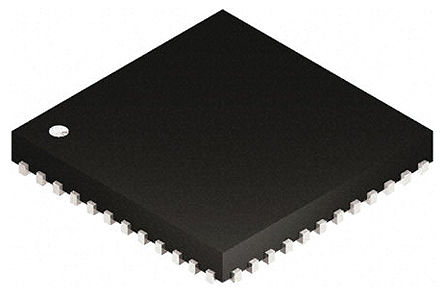
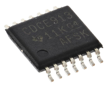
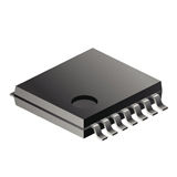
CDCE925PW
TEXAS INSTRUMENTS CDCE925PW 芯片, 可编程时钟合成器, 2锁相环, VCXO
The CDCE925 and CDCEL925 are modular PLL-based low-cost, high-performance, programmable clock synthesizers, multipliers, and dividers. They generate up to five output clocks from a single input frequency. Each output can be programmed in-system for any clock frequency up to 230 MHz, using up to two independent configurable PLLs.
The CDCEx925 has a separate output supply pin, VDDOUT, which is 1.8 V for CDCEL925 and 2.5 V to 3.3 V for CDCE925.
The input accepts an external crystal or LVCMOS clock signal. In case of a crystal input, an on-chip load capacitor is adequate for most applications. The value of the load capacitor is programmable from 0 to 20 pF. Additionally, an on-chip VCXO is selectable which allows synchronization of the output frequency to an external control signal, that is, PWM signal.
The deep M/N divider ratio allows the generation of zero-ppm audio/video, networking WLAN, Bluetooth, Ethernet, GPS, or interface USB, IEEE1394, memory stick clocks from a 27-MHz reference input frequency, for example.
All PLLs support SSC spread-spectrum clocking. SSC can be center-spread or down-spread clocking, which is a common technique to reduce electromagnetic interference EMI.
Based on the PLL frequency and the divider settings, the internal loop filter components are automatically adjusted to achieve high stability and optimized jitter transfer characteristic of each PLL.
The device supports nonvolatile EEPROM programming for easy customization of the device in the application. It is preset to a factory default configuration and can be reprogrammed to a different application configuration before it goes onto the PCB or reprogrammed by in-system programming. All device settings are programmable through the SDA/SCL bus, a 2-wire serial interface.
Three, free programmable control inputs, S0, S1, and S2, can be used to select different frequencies, or change the SSC setting for lowering EMI, or other control features like outputs disable to low, outputs in high-impedance state, power down, PLL bypass, and so forth.
The CDCx925 operates in a 1.8-V environment and in a temperature range of –40°C to 85°C.

