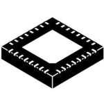
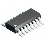
MC100EP195FAG
ON SEMICONDUCTOR MC100EP195FAG 芯片, 逻辑芯片 - ECL, 可编程延时器
NECL/PECL input transition.The delay section consists of a programmable matrix of gates and multiplexers as shown in the data sheet logic diagram. The delay increment of the EP195 has a digitally selectable resolution of about 10 ps and a range of up to 10.2 ns. The required delay is selected by the 10 data select inputs D0:9 which are latched on chip by a high signal on the latch enable LEN control. The MC10/100EP195 is a programmable delay chip PDC designed primarily for clock deskewing and timing adjustment. It provides variable delay of a differential The approximate delay values for varying tap numbers correlating to D0 LSB through D9 MSB are shown in the data sheet.Because the EP195 is designed using a chain of multiplexers it has a fixed minimum delay of 2.2 ns. An additional pin D10 is provided for cascading multiple PDCs for increased programmable range. The cascade logic allows full control of multiple PDCs. Select input pins D0-D10 may be threshold controlled by combinations of interconnects between V pin 8 for CMOS, ECL, or TTL level signals. For CMOS input levels, leave V open. For ECL operation, short V pins 7 and 8. For TTL level operation, connect a 1.5 V supply reference to V pin. The 1.5 V reference voltage to V pin can be accomplished by placing a 1.5k Ohm or 500 Ohm resistor between V for 3.3 V or 5.0 V power supplies, respectively. pin, an internally generated voltage supply, is available to this device only. For single-ended input conditions, the unused differential input is connected to V as a switching reference voltage. V may also rebias AC coupled inputs. When used, decouple V via a 0.01 uF capacitor and limit current sourcing or
Features
---
|
- .
- Maximum Frequency > 1.2 Ghz Typical
- .
- Programmable Range: 2.2 ns to 12.2 ns
- .
- 10 ps Increments
- .
- PECL Mode Operating Range: VCC = 3.0 V with VEE = 0 V
- .
- NECL Mode Operating Range: VCC = 0 V with VEE = -3.0 V
- .
- Open Input Default State
- .
- Safety Clamp on Inputs
- .
- A Logic High on the ENbar Pin Will Force Q to Logic Low
- .
- D[0:10] Can Accept Either ECL, CMOS, or TTL Inputs.
- .
- VBB Output Reference Voltage
- .
- Pb-Free Packages are Available