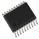
MC10EP139DTR2G
3.3V / 5V ECL ± 2/4, ±4 /5/6时钟发生器芯片 3.3V / 5V ECL ±2/4, ±4/5/6 Clock Generation Chip
The MC10/100EP139 is a low skew divide by 2/4, divide by 4/5/6 clock generation chip designed explicitly for low skew clock generation applications. The internal dividers are synchronous to each other, therefore, the common output edges are all precisely aligned. The device can be driven by either a differential or single-ended ECL or, if positive power supplies are used, LVPECL input signals. In addition, by using the V output, a sinusoidal source can be AC coupled into the device. If a single-ended input is to be used, the V output should be connected to the CLKbar input and bypassed to ground via a 0.01uF capacitor.The common enable ENbar is synchronous so that the internal dividers will only be enabled/disabled when the internal clock is already in the LOW state. This avoids any chance of generating a runt clock pulse on the internal clock when the device is enabled/disabled as can happen with an asynchronous control. The internal enable flip-flop is clocked on the falling edge of the input clock, therefore, all associated specification limits are referenced to the negative edge of the clock input. Upon startup, the internal flip-flops will attain a random state; therefore, for systems which utilize multiple EP139s, the master reset MR input must be asserted to ensure synchronization. For systems which only use one EP139, the MR pin need not be exercised as the internal divider design ensures synchronization between the divide by 2/4 and the divide by 4/5/6 outputs of a single device. All V pins must be externally connected to power supply to guarantee proper operation.The 100 Series contains temperature compensation.
Features
---
|
- .
- Maximum Frequency >1.0 GHz Typical
- .
- 50ps Output-to-Output Skew
- .
- PECL Mode Operating Range: VCC=3.0 V to 5.5 V with VEE = 0 V
- .
- NECL Mode Operating Range: VCC = 0 V with VEE = -3.0 V to -5.5 V
- .
- Open Input Default State
- .
- Safety Clamp on Inputs
- .
- Synchronous Enable/Disable
- .
- Master Reset for Synchronization of Multiple Chips
- .
- VBB Output
- .
- Pb-Free Packages are Available