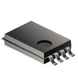
CDCS503TPWRQ1
时钟缓冲器/时钟乘法器具有可选SSC Clock Buffer/Clock Multiplier With Optional SSC
The CDCS503-Q1 device is a spread spectrum capable, LVCMOS input clock buffer with selectable frequency multiplication.
It shares major functionality with the CDCS502 but uses a LVCMOS input stage instead of the crystal input stage of the CDCS502, and the CDCS503-Q1 has an output enable pin.
The device accepts a 3.3-V LVCMOS signal at the input.
The input signal is processed by a phased-locked loop PLL, whose output frequency is either equal to the input frequency or multiplied by the factor of four.
The PLL is also able to spread the clock signal by ±0%, ±0.5%, ±1% or ±2% centered around the output clock frequency with a triangular modulation.
By this, the device can generate output frequencies between 8 MHz and 108 MHz with or without SSC.
A separate control pin can be used to enable or disable the output. The CDCS503-Q1 device operates in a 3.3-V environment.
It is characterized for operation from –40°C to 105°C, and available in an 8-pin TSSOP package.


