FDC6506P
数据手册.pdfFAIRCHILD SEMICONDUCTOR FDC6506P 双路场效应管, MOSFET, 双P沟道, 3 A, -30 V, 170 mohm, -10 V, -1.8 V
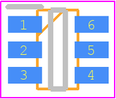
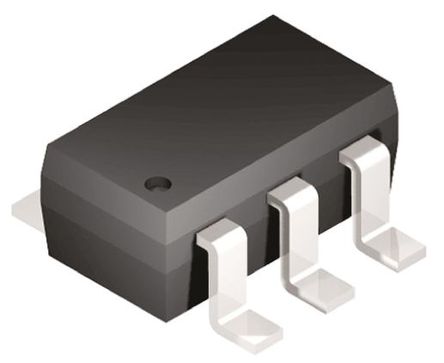
最大源漏极电压VdsDrain-Source Voltage| -30V \---|--- 最大栅源极电压Vgs±Gate-Source Voltage| -20V 最大漏极电流IdDrain Current| -1.8A 源漏极导通电阻RdsDrain-Source On-State Resistance| 280mΩ@ VGS = -4.5V, ID = -1.4A 开启电压Vgs(th)Gate-Source Threshold Voltage| -1~-3V 耗散功率PdPower Dissipation| 960mW/0.96W Description & Applications| Dual P-Channel Logic Level Power Trench MOSFET General Description These P-Channel logic level MOSFETs are produced using Semiconductor"s advanced Power Trench process that has been especially tailored to minimize on-state resistance and yet maintain low gate charge for superior switching performance. These devices have been designed to offer exceptional power dissipation in a very small footprint for applications where the bigger more expensive SO-8 and TSSOP-8 packages are impractical. Applications • Load switch • Battery protection • Power management Features • Low gate charge • Fast switching speed. • High performance trench technology for extremely low RDSON • Super SOTTM-6 package 描述与应用| 双P沟道逻辑电平功率沟槽MOSFET 概述 这些P沟道逻辑电平MOSFET采用飞兆半导体先进的功率沟槽进程,已特别是针对减少通态电阻,但维持出色的开关性能低栅极电荷。 这些设备已被设计为应用程序提供出色的功率耗散在一个非常小的足迹更大更昂贵的SO-8和TSSOP-8 包是不切实际。 应用 •负荷开关 •电池保护 •电源管理 特点 •低栅极电荷 •快速开关速度。 •高性能沟道技术极低的RDS(ON) •超级SOTTM-6封装