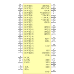
DS92LX2122SQE/NOPB
DS92LX2122SQE/NOPB 编带
The is a DC-balanced bi-directional control Deserializer Chipset offers a Channel Link III interface with a high-speed forward channel and a full-duplex control channel for data transmission over a single differential pair. It incorporates differential signalling on both the high-speed and bi-directional back channel control data paths. It is targeted for direct connections between graphics host controller and displays modules. This chipset is ideally suited for driving video data to displays requiring 18-bit colour depth RGB666 + HS, VS and DE along with a bi-directional back channel control bus. The primary transport converts 21 bit data over a single high-speed serial stream, along with a separate low latency bi-directional back channel transport that accepts control information from an I²C port. This single serial stream simplifies transferring a wide data bus over PCB traces and cable by eliminating the skew problems between parallel data and clock paths.
- .
- Supports 18-bit colour depth RGB666 + HS, VS, DE
- .
- Embedded clock with DC balanced coding to support AC-coupled interconnects
- .
- Capable to drive up to 10m shielded twisted-pair cable
- .
- Bi-directional control interface channel with I²C support
- .
- I²C interface for device configuration
- .
- Single-pin ID addressing
- .
- Up to 4 GPI on DES and GPO on SER
- .
- AT-SPEED BIST diagnosis feature to validate link integrity
- .
- Individual power-down controls for both Ser and Des
- .
- User-selectable clock edge for parallel data on both Ser and Des
- .
- Integrated termination resistors
- .
- No reference clock required
- .
- Programmable receive equalization
- .
- Lock output reporting pin to ensure
- .
- Up to 1050Mbps data throughput
- .
- 10 to 50MHz Input clock support
- .
- Green product and no Sb/Br