TPS1100D
单P沟道增强型MOSFET SINGLE P-CHANNEL ENHANCEMENT-MODE MOSFETS
The TPS1100 is a single P-channel enhancement-mode MOSFET. The device has been optimized for 3-V or 5-V power distribution in battery-powered systems by means of Texas Instruments LinBiCMOSTM process. With a maximum VGSth of -1.5 V and an IDSS of only 0.5 uA, the TPS1100 is the ideal high-side switch for low-voltage, portable battery-management systems where maximizing battery life is a primary concern. The low rDSon and excellent ac characteristics rise time 10 ns typical make the TPS1100 the logical choice for low-voltage switching applications such as power switches for pulse-width-modulated PWM controllers or motor/bridge drivers.
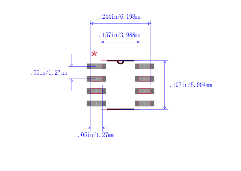
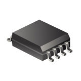
The ultrathin thin shrink small-outline package or TSSOP PW version with its smaller footprint and reduction in height fits in places where other P-channel MOSFETs cannot. The size advantage is especially important where board real estate is at a premium and height restrictions do not allow for a small-outline integrated circuit SOIC package.
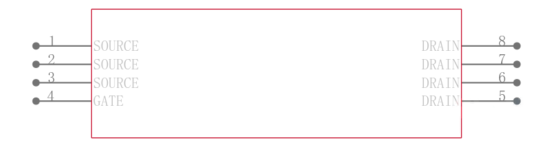
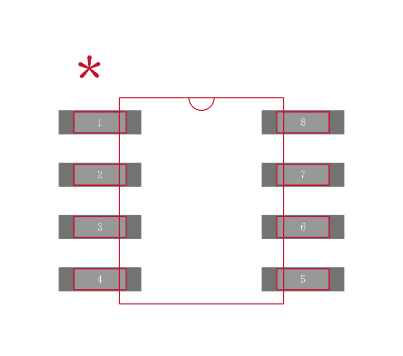
Such applications include notebook computers, personal digital assistants PDAs, cellular telephones, and PCMCIA cards. For existing designs, the D-packaged version has a pinout common with other p-channel MOSFETs in SOIC packages.
Caution. This device contains circuits to protect its inputs and outputs against damage due to high static voltages or electrostatic fields. These circuits have been qualified to protect this device against electrostatic discharges ESD of up to 2 kV according to MIL-STD-883C, Method 3015; however, it is advised that precautions be taken to avoid application of any voltage higher than maximum-rated voltages to these high-impedance circuits.
View datasheet View product folder