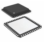
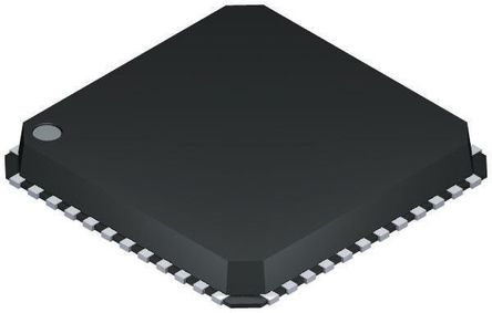
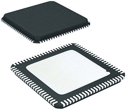
AD9528BCPZ-REEL7
PLL Clock Generator Dual 3450MHz to 4025MHz 72Pin LFCSP T/R
Product Details
The AD9528 is a two-stage PLL with an integrated JESD204B SYSREF generator for multiple device synchronization. The first stage phase-locked loop PLL PLL1 provides input reference conditioning by reducing the jitter present on a system clock. The second stage PLL PLL2 provides high frequency clocks that achieve low integrated jitter as well as low broadband noise from the clock output drivers. The external VCXO provides the low noise reference required by PLL2 to achieve the restrictive phase noise and jitter requirements necessary to achieve acceptable performance. The on-chip VCO tunes from 3.450 GHz to 4.025 GHz. The integrated SYSREF generator outputs single shot, N-shot, or continuous signals synchronous to the PLL1 and PLL2 outputs to time align multiple devices.
The AD9528 generates two outputs Output 1 and Output 2 with a maximum frequency of 1.25 GHz, and 12 outputs up to 1 GHz. Each output can be configured to output directly from PLL1, PLL2, or the internal SYSREF generator. Each of the 14 output channels contains a divider with coarse digital phase adjustment and an analog fine phase delay block that allows complete flexibility in timing alignment across all 14 outputs. The AD9528 can also be used as a dual input flexible buffer to distribute 14 device clock and/or SYSREF signals. At power-up, the AD9528 sends the VCXO signal directly to Output 12 and Output 13 to serve as the power-up ready clocks.
Note that, throughout this data sheet, the dual function pin names are referenced by the relevant function where applicable.
**Applications**
- .
- High performance wireless transceivers
- .
- LTE and multicarrier GSM base stations
- .
- Wireless and broadband infrastructure
- .
- Medical instrumentation
- .
- Clocking high speed ADCs, DACs, DDSs, DDCs, DUCs, MxFEs; supports JESD204B
- .
- Low jitter, low phase noise clock distribution
- .
- ATE and high performance instrumentation
### Features and Benefits
- .
- 14 outputs configurable for HSTL or LVDS
- .
- Maximum output frequency
2 outputs up to 1.25 GHz
12 outputs up to 1 GHz
- .
- Dependent on the voltage controlled crystal oscillator
VCXO frequency accuracy start-up frequency accuracy: <±100 ppm
- .
- Dedicated 8-bit dividers on each output
Coarse delay: 63 steps at 1/2 the period of the RF VCO divider output frequency with no jitter impact
Fine delay: 15 steps of 31 ps resolution
- .
- Typical output-to-output skew: 20 ps
- .
- Duty cycle correction for odd divider settings
- .
- Output 12 and Output 13, VCXO output at power-up
- .
- Absolute output jitter: <160 fs at 122.88 MHz
12 kHz to 20 MHz Integration range
- .
- See data sheet for additional features