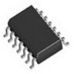
LTC2052HVCS#PBF
LINEAR TECHNOLOGY LTC2052HVCS#PBF 运算放大器, 四路, 3 MHz, 4个放大器, 2 V/µs, 2.7V 至 ± 5.5V, SOIC, 14 引脚
The is a quad zero-drift Operational Amplifier operates from a single 2.7V supply and support ±5V applications. The current consumption is 750µA per op amp. The LTC2052, despite their miniature size, feature uncompromising DC performance. The typical input offset voltage and offset drift is 0.5µV and 10nV/°C. The almost zero DC offset and drift are supported with a power supply rejection ratio PSRR and common mode rejection ratio CMRR of more than 130dB. The input common mode voltage ranges from the negative supply up to typically 1V from the positive supply. The LTC2052 have an enhanced output stage capable of driving loads as low as 2kR to both supply rails. The open-loop gain is typically 140dB. The LTC2052 feature a 1.5µVP-P DC to 10Hz noise and a 3MHz gain-bandwidth product.
- .
- 3µV Maximum offset voltage
- .
- 30nV/°C Maximum offset voltage drift
- .
- 1.5µVP-P 0.01Hz to 10Hz typical Noise
- .
- 140dB typical Voltage gain
- .
- 130dB typical PSRR
- .
- 130dB typical CMRR
- .
- 0.75mA typical Per amplifier supply current
- .
- Extended common mode input range
- .
- Output swings rail-to-rail