ADN4670
可编程低压1:10 LVDS时钟驱动器 Programmable Low Voltage 1:10 LVDS Clock Driver
GENERAL DESCRIPTION
The is a low voltage differential signaling LVDS clock driver that expands a differential clock input signal to 10 differential clock outputs. The device is programmable using a simple serial interface, so that one of two clock inputs can be selected CLK0/CLK0 or CLK1/CLK1 and any of the differential outputs Q0/Q0 to Q9/Q9 can be enabled or disabled tristated. The ADN4670 is designed for use in 50 Ω transmission line environments.
When the enable input EN is high, the device may be programmed by clocking 11 data bits into the shift register. The first 10 bits determine which outputs are enabled 0 = disabled, 1 = enabled, while the 11th bit selects the clock input 0 = CLK0, 1 = CLK1. A 12th clock pulse transfers data from the shift register to the control register.
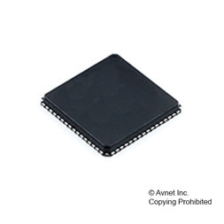
The ADN4670 is fully specified over the industrial temperature range and is available in a 32-lead LFCSP and LQFP packages.
FEATURES
Low output skew <30 ps typical
Distributes one differential clock input to 10 LVDS clock outputs
Programmable—one of two differential clock inputs can be selected CLK0, CLK1 and individual differential clock outputs enabled/disabled
Signaling rate up to 1.1 GHz typical
2.375 V to 2.625 V power supply range
±100 mV differential input threshold
Input common-mode range from rail-to-rail
I/O pins fail-safe during power-down: VDD = 0 V
Available in 32-lead LFCSP and LQFP packages
Industrial operating temperature range: −40°C to +85°C
APPLICATIONS
Clock distribution networks