AD9574BCPZ-REEL7
时钟发生器及支持产品 Enterprise network clock chipw/ crystal
Product Details
The AD9574 provides a multiple output clock generator function comprising a dedicated phase-locked loop PLL core optimized for Ethernet and gigabit Ethernet line card applications. The integer-N PLL design is based on the Analog Devices, Inc., proven portfolio of high performance, low jitter frequency synthesizers to maximize network performance. The AD9574 also benefits other applications requiring low phase noise and jitter performance.
Configuring the AD9574 for a particular application requires only the connection of external pull-up or pull-down resistors to the appropriate pin program reader pins PPRx. These pins provide control of the internal dividers for establishing the desired frequency translations, clock output functionality, and input reference functionality. Connecting an external 19.44 MHz or 25 MHz oscillator to one or both of the REF0_P/REF0_N or REF1_P/REF1_N reference inputs results in a set of output frequencies prescribed by the PPRx pins. Connecting a stable clock source 8 kHz/10 MHz/19.44 MHz/25 MHz/38.88 MHz to the monitor clock input enables the optional monitor circuit providing quality of service QoS status for REF0 or REF1.
The PLL section consists of a low noise phase frequency detector PFD, a precision charge pump CP, a partially integrated loop filter LF, a low phase noise voltage controlled oscillator VCO, and feedback and output dividers. The divider values depend on the PPRx pins. The integrated loop filter requires only a single external capacitor connected to the LF pin.
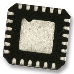
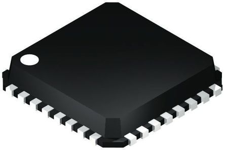
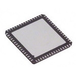
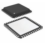
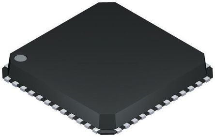
The AD9574 is packaged in a 48-lead 7 mm × 7 mm LFCSP, requiring only a single 3.3 V supply. The operating temperature range is −40°C to +85°C.
**Applications**
- .
- Ethernet line cards, switches, and routers
- .
- SATA and PCI express
- .
- Low jitter, low phase noise clock generation
### Features and Benefits
- .
- Redundant input reference clock capability
- .
- Reference monitoring function
- .
- Fully integrated VCO/PLL core
- .
- Jitter rms
- .
- 0.234 ps rms jitter 10 kHz to 10 MHz at 156.25 MHz
- .
- 0.243 ps rms jitter 12 kHz to 20 MHz at 156.25 MHz
- .
- Input frequency: 19.44 MHz or 25 MHz
- .
- Preset frequency translations
- .
- Using a 19.44 MHz input reference
- .
- 19.44 MHz, 38.88 MHz, 77.76 MHz, 155.52 MHz
- .
- Using a 25 MHz input reference
- .
- 25 MHz, 33.33 MHz, 50 MHz, 66.67 MHz, 80 MHz, 100 MHz, 125 MHz, 133.3 MHz, 156.25 MHz, 160 MHz, 312.5 MHz
- .
- Output drive formats: HSTL, LVDS, HCSL, and 1.8 V and 3.3 V CMOS
- .
- Integrated loop filter requires a single external capacitor
- .
- 2 copies of reference clock output
- .
- Device configuration via strapping pins PPRx
- .
- Space-saving 7 mm × 7 mm 48-lead LFCSP
- .
- 3.3 V operation