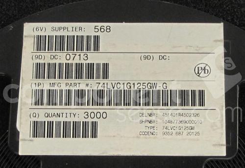
74LVC1G74GM
单一的D- FL型IP- FL运算与置位和复位;上升沿触发 Single D-type flip-flop with set and reset; positive edge trigger
General description
The 74LVC1G74 is a single positive edge triggered D-type flip-flop with individual data D
inputs, clock CP inputs, set SD and reset RD inputs, and complementary Q and Q
outputs.
This device is fully specified for partial power-down applications using IOFF. The IOFF circuitry disables the output, preventing damaging backflow current through the device when it is powered down.
The set and reset are asynchronous active LOW inputs and operate independently of the clock input. Information on the data input is transferred to the Q output on the LOW-to-HIGH transition of the clock pulse. The D inputs must be stable one set-up time prior to the LOW-to-HIGH clock transition for predictable operation.
Schmitt trigger action at all inputs makes the circuit highly tolerant of slower input rise and
fall times.
Features and benefits
Wide supply voltage range from 1.65 V to 5.5 V
5 V tolerant inputs for interfacing with 5 V logic
High noise immunity
Complies with JEDEC standard:
JESD8-7 1.65 V to 1.95 V
JESD8-5 2.3 V to 2.7 V
JESD8-B/JESD36 2.7 V to 3.6 V
ESD protection:
HBM JESD22-A114F exceeds 2000 V
MM JESD22-A115-A exceeds 200 V
±24 mA output drive VCC=3.0V
CMOS low power consumption
Latch-up performance exceeds 250 mA
Direct interface with TTL levels
Inputs accept voltages up to 5 V
Multiple package options
Specified from -40F℃ to +85℃ and 40℃ to +125℃