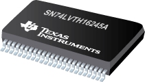
SN74LVTH16245A
具有三态输出的 3.3V ABT 16 位总线收发器
* Members of the Texas Instruments Widebus Family
- .
- State-of-the-Art Advanced BiCMOS Technology ABT Design for 3.3-V Operation and Low Static-Power Dissipation
- .
- Support Mixed-Mode Signal Operation 5-V Input and Output Voltages With 3.3-V VCC
- .
- Support Unregulated Battery Operation Down to 2.7 V
- .
- Typical VOLP Output Ground Bounce <0.8 V at VCC = 3.3 V, TA = 25°C
- .
- Distributed VCC and GND Pins Minimize High-Speed Switching Noise
- .
- Flow-Through Architecture Optimizes PCB Layout
- .
- Ioff and Power-Up 3-State Support Hot Insertion
- .
- Bus Hold on Data Inputs Eliminates the Need for External Pullup/Pulldown Resistors
- .
- Latch-Up Performance Exceeds 500 mA Per JESD 17
- .
- ESD Protection Exceeds JESD 22
- .
- 2000-V Human-Body Model A114-A
- .
- 200-V Machine Model A115-A
Widebus is a trademark of Texas Instruments.
## DESCRIPON/ORDERING INFORMATION
The "LVTH16245A devices are 16-bit dual-octal noninverting 3-state transceivers designed for low-voltage 3.3-V VCC operation, but with the capability to provide a TTL interface to a 5-V system environment.
The devices are designed for asynchronous communication between two data buses. The logic levels of the direction-control DIR input and the output-enable OE input activate either the B-port outputs or the A-port outputs or place both output ports into the high-impedance mode. The device transmits data from the A bus to the B bus when the B-port outputs are activated, and from the B bus to the A bus when the A-port outputs are activated. The input circuitry on both A and B ports is always active and must have a logic HIGH or LOW level applied to prevent excess ICC and ICCZ.
Active bus-hold circuitry holds unused or undriven inputs at a valid logic state. Use of pullup or pulldown resistors with the bus-hold circuitry is not recommended.
When VCC is between 0 and 1.5 V, the devices are in the high-impedance state during power up or power down. However, to ensure the high-impedance state above 1.5 V, OE should be tied to VCC through a pullup resistor; the minimum value of the resistor is determined by the current-sinking capability of the driver.
These devices are fully specified for hot-insertion applications using Ioff and power-up 3-state. The Ioff circuitry disables the outputs, preventing damaging current backflow through the devices when they are powered down. The power-up 3-state circuitry places the outputs in the high-impedance state during power up and power down, which prevents driver conflict.

