ADN2819
多速率为2.7 Gb / s的时钟和数据恢复IC,集成限幅放大器 Multirate to 2.7 Gb/s Clock and Data Recovery IC with Integrated Limiting Amp
Product Details
The provides receiver functions of Quantization, Signal Level Detect and Clock and Data Recovery at rates of OC-3, OC-12, Gigabit Ethernet, OC-48 and all FEC rates. All SONET jitter requirements are met, including: Jitter Transfer; Jitter Generation; and Jitter Tolerance. All specifications are quoted for -40ºC to +85ºC ambient temperature unless otherwise noted.
The proprietary delay and phase-locked loop design of the ADN2819 provides unprecedented jitter performance for robust high-speed networking designs.
The device is intended for WDM system applications and can be used with either an external reference clock or an on-chip crystal oscillator. Both native rates and 15/14 rate digital wrappers rates are supported by the ADN2819, without any change of reference clock required. This device together with a PIN diode and a TIA preamplifier can implement a highly integrated, low cost, low power fiber optic receiver. The receiver front end Signal Detect circuit indicates when the input signal level has fallen below a user adjustable threshold.
### Features and Benefits
- .
- Multirate 155/166 Mbps, 622/666 Mbps, 1.25/1.34 Gbps, 2.49/2.67 Gbps
- .
- Integrated Limiting Amplifier with Adjustable Slice
- .
- Quantizer Sensitivity: 6 mV
- .
- Adjustable Slice Level: ±100 mV
- .
- Exceeds all SONET/SDH Requirements for Jitter Transfer, Generation, and Tolerance
- .
- Internal MUX to Bypass CDR
- .
- Low power: 540 mW
- .
- One supply: 3.0V - 3.6V
- .
- Single Reference Clock Frequency for All Rates
- .
- Loss-of-Lock Indicator
- .
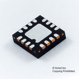
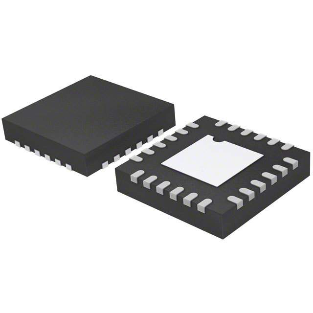
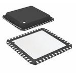
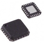
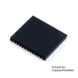
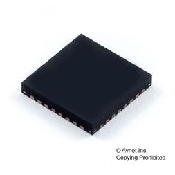
- Small Footprint: 48-lead LFCSP Package 7 mm x 7 mm overall