CDCLVD2108RGZT
双1 : 8低附加抖动LVDS缓冲器 Dual 1:8 Low Additive Jitter LVDS Buffer
The CDCLVD2108 clock buffer distributes two clock inputs IN0, IN1 to a total of 16 pairs of differential LVDS clock outputs OUT0, OUT15. Each buffer block consists of one input and 8 LVDS outputs. The inputs can either be LVDS, LVPECL, or LVCMOS.
The CDCLVD2108 is specifically designed for driving 50- transmission lines. In case of driving the inputs in single ended mode, the appropriate bias voltage VAC_REF should be applied to the unused negative input pin.
Using the control pin EN outputs can be either disabled or enabled. If the EN pin is left open all outputs are active, if switched to a logical "0" all outputs are disabled static logical 0, if switched to a logical "1", OUT 8..15 are switched off and OUT 0..7 are active. The part supports a fail safe function. It incorporates an input hysteresis, which prevents random oscillation of the outputs in absence of an input signal.
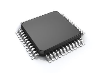
The device operates in 2.5V supply environment and is characterized from –40°C to 85°C ambient temperature. The CDCLVD2108 is packaged in small 48-pin, 7-mm × 7-mm QFN package.