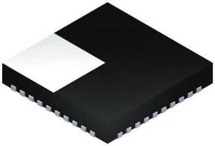
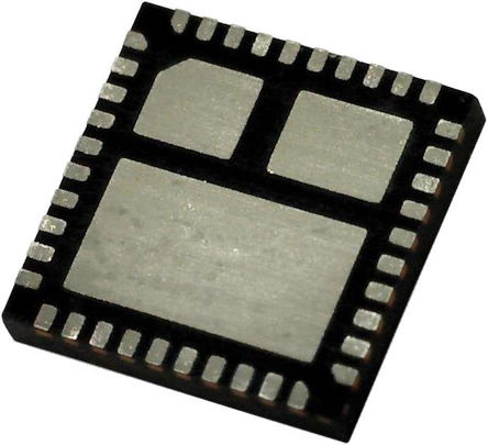
FDMF5821
FDMF5821: 带集成温度监控器的智能功率级 SPS 模块
The SPS family is ON’s next-generation, fully optimized, ultra-compact, integrated MOSFET plus driver power stage solution for high-current, high-frequency, synchronous buck, DC-DC applications. The integrates a driver IC with a bootstrap Schottky diode, two power MOSFETs, and a thermal monitor into a thermally enhanced, ultra-compact, 5 mm x 5 mm package.With an integrated approach, the SPS switching power stage is optimized for driver and MOSFET dynamic performance, minimized system inductance, and power MOSFET RDSON. The SPS family uses Fairchild"s high-performance PowerTrench® MOSFET technology, which reduces switch ringing, eliminating the need for a snubber circuit in most buck converter applications.A driver IC with reduced dead times and propagation delays further enhances the performance. A thermal monitor function warns of a potential over-temperature situation. A programmable thermal shutdown function turns off the driver if an over-temperature condition occurs. The FDMF5821 incorporates an Auto-DCM Mode ZCD# for improved light-load efficiency. The FDMF5821 also provides a 3-state 5 V PWM input for compatibility with a wide range of PWM controllers.
Features
---
|
- .
- Ultra-Compact 5 mm x 5 mm PQFN Copper-Clip Package with Flip Chip Low-Side MOSFET
- .
- High Current Handling: 60 A
- .
- 3-State 5 V PWM Input Gate Driver
- .
- Dynamic Resistance Mode for Low-Side Drive LDRV Slows Low-Side MOSFET during Negative Inductor Current Switching
- .
- Auto DCM Low-Side Gate Turn Off Using ZCD# Input
- .
- Thermal Monitor for Module Temperature Reporting
- .
- Programmable Thermal Shutdown P_THDN
- .
- HS-Short Detect Fault# / Shutdown
- .
- Dual Mode Enable / Fault# Pin
- .
- Internal Pull-Up and Pull-Down for ZCD# and EN Inputs, respectively
- .
- ON’s PowerTrench® MOSFETs for Clean Voltage Waveforms and Reduced Ringing
- .
- ON’s SyncFET™ Technology Integrated Schottky Diode in Low-Side MOSFET
- .
- Integrated Bootstrap Schottky Diode
- .
- Optimized / Extremely Short Dead-Times
- .
- Optimized for Switching Frequencies up to 1.5 MHz
- .
- Under-Voltage Lockout UVLO on VCC
- .
- Low Shutdown Current: < 3 μA
- .
- PWM Minimum Controllable On-Time: 30 ns
- .
- Operating Junction Temperature Range: -40°C to +125°C
- .
- Optimized FET Pair for Highest Efficiency: 10 ~ 15% Duty Cycle
- .
- ON Green Packaging and RoHS Compliance