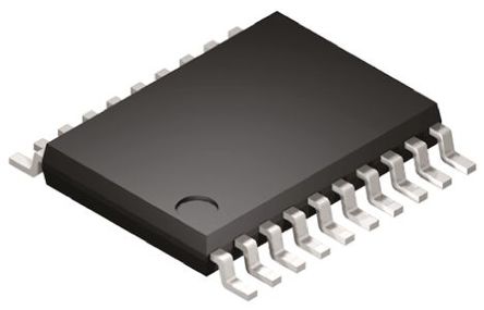
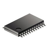
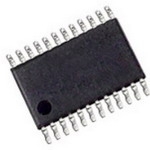
NB3N51044DTR2G
NB3N51044: 时钟产生器,3.3 V,晶振至 100 MHz / 125MHz,四路 HCSL / LVDS
The NB3N51044 is a precision, low phase noise clock generator that supports PCI Express and sRIO clock requirements. The device accepts a 25 MHz fundamental mode parallel resonant crystal or a 25 MHz single ended reference clock signal and generates four differential HCSL/LVDS outputs of 100 MHz or 125 MHz clock frequency based on frequency select input F_SEL. NB3N51044 is configurable to bypass the PLL from signal path using BYPASS, and provides the output frequency through the divider network. All clock outputs can be individually enabled / disabled through hardware input pins OE. In addition, device can be reset using Master Reset input pin MR_OE#.
Features | | Benefits
---|---|---
| | | | |
- .
- Output frequency selection of 100 MHz or 125 MHz
| |
- .
- PCIe and sRIO compliant
- .
- Typical Phase Jitter @ 125 MHz integrated 1.875 MHz to 20 MHz: 0.2 ps
| |
- .
- Best in Class Jitter Performance
- .
- Typical Cycle-cycle Jitter @ 100 MHz 10k cycles: 20 ps
| |
- .
- Best in Class Jitter Performance
- .
- Uses 25 MHz Fundamental Crystal or Reference Clock Input
| |
- .
- Four Low Skew HCSL or LVDS Outputs
| |
- .
- Individual OE Tri-states Output
| |
- .
- Master Reset and BYPASS modes
| |
- .
- PCIe Gen 1, Gen 2, Gen 3 Compliant
| |
- .
- Operating Supply Voltage Range 3.3 V ± 5%
| |
- .
- Industrial Temperature Range-40°C to +85°C
| |