TMS320DM335
数字媒体片上系统 DMSoC
The DM335 processor is a low-cost, low-power processor providing advanced graphical user interface for display applications that do not require video compression and decompression. Coupled with a video processing subsystem VPSS that provides 720p display, the DM335 processor is powered by a 135/216-MHz ARM926EJ-S core so developers can create feature-rich graphical user interfaces allowing customers to interact with their portable, electronic devices such as video-enabled universal remote controls, Internet radio, e-books, video doorbells, and digital telescopes. The new DM335 is packed with the same peripherals as its predecessor, the TMS320DM355 device, including high-speed USB 2.0 on-the-go, external memory interface EMIF, mobile DDR/DDR2, two SDIO ports, three UART Ports, two Audio Serial Ports, three SPI Ports, and SLC/MCL NAND Flash memory support. These peripherals help customers create DM335 processor-based designs that add video and audio excitement to a wide range of today"s static user-interface applications while keeping silicon costs and power consumption low. The new digital media processor is completely scalable with the DM355 processor and Digital Video Evaluation Board DVEVM, allowing customers to utilize their same code for their new DM335 processor focused designs.
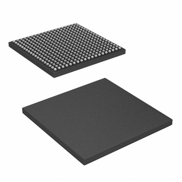
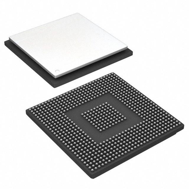
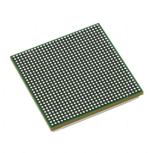
The new DM335 device delivers a sophisticated suite of capabilities allowing for flexible image capture and display. Through its user interface technology, such as a four-level on-screen display, developers are able to create picture-within-picture and video-within-video as well as innovative graphic user interfaces. This is especially important for portable products that require the use of button or touch screen, such as portable karaoke, video surveillance and electronic gaming applications. Additional advanced capture and imaging technologies include support for CCD/CMOS image sensors, resize capability and video stabilization. The 1280-by-960-pixel digital LCD connection runs on a 75-MHz pixel clock and supports TV composite output for increased expandability. This highly integrated device is packaged in a 13 x 13 mm, 337 pin , 0.65 mm pitch BGA package.
The DM335 processor core is an ARM926EJ-S RISC processor. The ARM926EJ-S is a 32-bit processor core that performs 32-bit and 16-bit instructions and processes 32-bit, 16-bit, and 8-bit data. The core uses pipelining so that all parts of the processor and memory system can operate continuously. The ARM core incorporates:
- .
- A coprocessor 15 CP15 and protection module
- .
- Data and program Memory Management Units MMUs with table look-aside buffers.
- .
- Separate 16K-byte instruction and 8K-byte data caches. Both are four-way associative with virtual index virtual tag VIVT.
The DM335 device has a Video Processing Subsystem VPSS with two configurable video/imaging peripherals:
- .
- A Video Processing Front-End VPFE
- .
- A Video Processing Back-End VPBE
The VPFE port provides an interface for CCD/CMOS imager modules and video decoders. The VPBE provides hardware On Screen Display OSD support and composite NTSC/PAL and digital LCD output.
The DM335 peripheral set includes:
- .
- An inter-integrated circuit I2C Bus interface
- .
- Two audio serial ports ASP
- .
- Three 64-bit general-purpose timers each configurable as two independent 32-bit timers
- .
- A 64-bit watchdog timer
- .
- Up to 104-pins of general-purpose input/output GPIO with programmable interrupt/event generation modes, multiplexed with other peripherals
- .
- Three UARTs with hardware handshaking support on one UART
- .
- Three serial port Interfaces SPI
- .
- Four pulse width modulator PWM peripherals
- .
- Four real time out RTO outputs
- .
- Two Multi-Media Card / Secure Digital MMC/SD/SDIO interfaces
- .
- Wireless interfaces Bluetooth, WLAN, WUSB through SDIO
- .
- A USB 2.0 full and high-speed device and host interface
- .
- Two external memory interfaces:
- .
- An asynchronous external memory interface AEMIF for slower memories/peripherals such as NAND and OneNAND,
- .
- A high speed synchronous memory interface for DDR2/mDDR.
For software development support the DM335 has a complete set of ARM development tools which include: C compilers, assembly optimizers to simplify programming and scheduling, and a Windows™debugger interface for visibility into source code execution.
- .
- Highlights
- .
- High-Performance Digital Media System-On-Chip DMSoC
- .
- Up to 216-MHz ARM926EJ-STM Clock Rate
- .
- Digital HDTV 720p/1080i output for connection to external encoder
- .
- Video Processing Subsystem
- .
- Hardware IPIPE for Real-Time Image Processing
- .
- Up to 14-bit CCD/CMOS Digital Interface
- .
- Histogram Module
- .
- Resize Image 1/16x to 8x
- .
- Hardware On-Screen Display
- .
- Up to 75-MHz Pixel Clock
- .
- Composite NTSC/PAL video encoder output
- .
- Peripherals include DDR and mDDR SDRAM, 2 MMC/SD/SDIO and SmartMedia Flash Card Interfaces, USB 2.0, 3 UARTs and 3 SPIs
- .
- Enhanced Direct-Memory-Access EDMA
- .
- Configurable Power-Saving Modes
- .
- On-Chip ARM ROM Bootloader RBL to Boot From NAND Flash, MMC/SD, or UART
- .
- 3.3-V and 1.8-V I/O, 1.3-V Core
- .
- Debug Interface Support
- .
- Up to 104 General-Purpose I/O GPIO Pins
- .
- 337-Pin Ball Grid Array at 65 nm Process Technology
* High-Performance Digital Media System-on-Chip
- .
- 135-, 216-MHz ARM926EJ-S™ Clock Rate
- .
- Fully Software-Compatible With ARM™
- .
- Extended Temperature 135- and 216-MHz Devices are Available
* ARM926EJ-S Core
- .
- Support for 32-Bit and 16-Bit Thumb Mode Instruction Sets
- .
- DSP Instruction Extensions and Single Cycle MAC
- .
- ARM® Jazelle® Technology
- .
- EmbeddedICE-RT™ Logic for Real-Time Debug
* ARM9 Memory Architecture
- .
- 16K-Byte Instruction Cache
- .
- 8K-Byte Data Cache
- .
- 32K-Byte RAM
- .
- 8K-Byte ROM
- .
- Little Endian
* Video Processing Subsystem
- .
- Front End Provides:
- .
- Hardware IPIPE for Real-Time Image Processing
- .
- Up to 14-bit CCD/CMOS Digital Interface
- .
- 16-/8-bit Generic YcBcR-4:2 Interface BT.601
- .
- 10-/8-bit CCIR6565/BT655 Interface
- .
- Up to 75-MHz Pixel Clock
- .
- Histogram Module
- .
- Resize Engine
- .
- Resize Images From 1/16x to 8x
- .
- Separate Horizontal/Vertical Control
- .
- Two Simultaneous Output Paths
- .
- Back End Provides:
- .
- Hardware On-Screen Display OSD
- .
- Composite NTSC/PAL video encoder output
- .
- 8-/16-bit YCC and Up to 18-Bit RGB666 Digital Output
- .
- BT.601/BT.656 Digital YCbCr 4:2:2 8-/16-Bit Interface
- .
- Digital HDTV 720p/1080ioutput for connection to external encoder
* External Memory Interfaces EMIFs
- .
- DDR2 and mDDR SDRAM 16-bit wide EMIF With 256 MByte Address Space 1.8-V I/O
- .
- Asynchronous16-/8-bit Wide EMIF AEMIF
- .
- Flash Memory Interfaces
- .
- NAND 8-/16-bit Wide Data
- .
- OneNAND16-bit Wide Data
* Flash Card Interfaces
- .
- Two Multimedia Card MMC / Secure Digital SD/SDIO
- .
- SmartMedia
* Enhanced Direct-Memory-Access EDMA Controller 64 Independent Channels
* USB Port with Integrated 2.0 High-Speed PHY that Supports
- .
- USB 2.0 Full and High-Speed Device
- .
- USB 2.0 Low, Full, and High-Speed Host
* Three 64-Bit General-Purpose Timers each configurable as two 32-bit timers
* One 64-Bit Watch Dog Timer
* Three UARTs One fast UART with RTS and CTS Flow Control
* Three Serial Port Interfaces SPI each with two Chip-Selects
* One Master/Slave Inter-Integrated Circuit I2C Bus®
* Two Audio Serial Port ASP
- .
- I2S and TDM I2S
- .
- AC97 Audio Codec Interface
- .
- S/PDIF via Software
- .
- Standard Voice Codec Interface AIC12
- .
- SPI Protocol Master Mode Only
* Four Pulse Width Modulator PWM Outputs
* Four RTO Real Time Out Outputs
* Up to 104 General-Purpose I/O GPIO Pins Multiplexed with Other Device Functions
* On-Chip ARM ROM Bootloader RBL to Boot From NAND Flash, MMC/SD, or UART
* Configurable Power-Saving Modes
* Crystal or External Clock Input typically 24 MHz or 36 MHz
* Flexible PLL Clock Generators
* Debug Interface Support
- .
- IEEE-1149.1 JTAG Boundary-Scan-Compatible
- .
- ETB™ Embedded Trace Buffer™ with4K-Bytes Trace Buffer memory
- .
- Device Revision ID Readable by ARM
* 337-Pin Ball Grid Array BGA Package ZCE Suffix, 0.65-mm Ball Pitch
* 90nm Process Technology
* 3.3-V and 1.8-V I/O, 1.3-V Internal
* Community Resources
- .
- E2E Community
- .
- TI Embedded Processors Wiki
Windows is a trademark of Microsoft.
All other trademarks are the property of their respective owners.