CY7C2170KV18-400BZC
静态随机存取存储器 18MB 512Kx36 1.8v 400MHz DDR II 静态随机存取存储器
Functional Description
The CY7C2168KV18, and CY7C2170KV18 are 1.8 V Synchronous Pipelined SRAMs equipped with DDR II+ architecture. The DDR II+ consists of an SRAM core with advanced synchronous peripheral circuitry. Addresses for read and write are latched on alternate rising edges of the input K clock. Write data is registered on the rising edges of both K and K. Read data is driven on the rising edges of K and K. Each address location is associated with two 18-bit words CY7C2168KV18, or 36-bit words CY7C2170KV18 that burst sequentially into or out of the device.
Features
■ 18-Mbit density 1 M × 18, 512 K × 36
■ 550-MHz clock for high bandwidth
■ Two-word burst for reducing address bus frequency
■ Double data rate DDR interfaces data transferred at 1100 MHz at 550 MHz
■ Available in 2.5 clock cycle latency
■ Two input clocks K and K for precise DDR timing
❐ SRAM uses rising edges only
■ Echo clocks CQ and CQ simplify data capture in high-speed systems
■ Data valid pin QVLD to indicate valid data on the output
■ On-die termination ODT feature
❐ Supported for D[x:0], BWS[x:0], and K/K inputs
■ Synchronous internally self-timed writes
■ DDR II+ operates with 2.5 cycle read latency when DOFF is asserted HIGH
■ Operates similar to DDR I device with one cycle read latency when DOFF is asserted LOW
■ Core VDD = 1.8 V ± 0.1 V; I/O VDDQ = 1.4 V to VDD[1]
❐ Supports both 1.5 V and 1.8 V I/O supply
■ HSTL inputs and variable drive HSTL output buffers
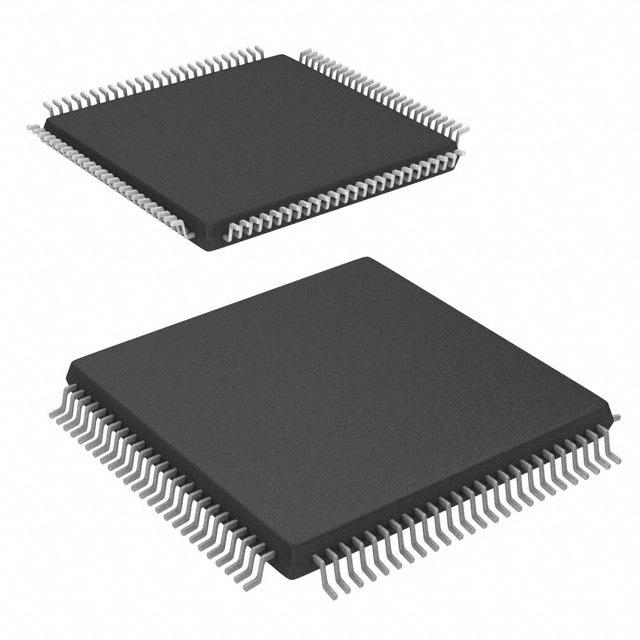
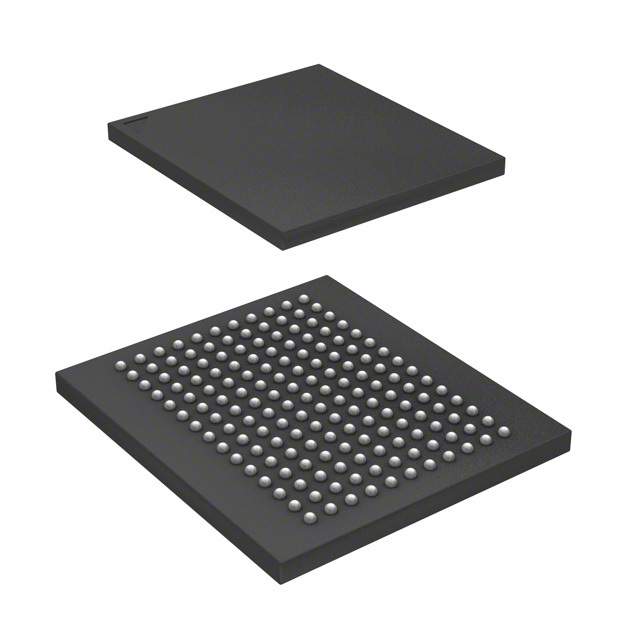
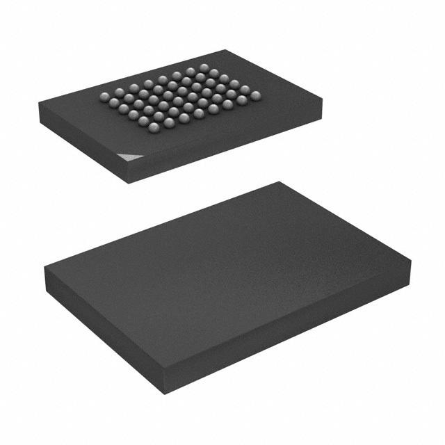
■ Available in 165-ball FBGA package 13 × 15 × 1.4 mm
■ CY7C2168KV18 offered in non Pb-free packages and CY7C2170KV18 offered in both Pb-free and non Pb-free packages
■ JTAG 1149.1 compatible test access port
■ Phase locked loop PLL for accurate data placement