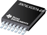
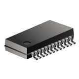
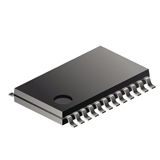
SN74LVC07A-EP
具有漏极开路输出的增强型产品六路缓冲器/驱动器
* Operates From 1.65 V to 5 V
- .
- Inputs and Open-Drain Outputs Accept Voltages up to 5.5 V
- .
- Max tpd of 3.6 ns at 5 V
- .
- Latch-Up Performance Exceeds 250 mA Per JESD 17
- .
- SUPPORTS DEFENSE, AEROSPACE, AND MEDICAL APPLICA ONS
- .
- Controlled Baseline
- .
- One Assembly/Test Site
- .
- One Fabrication Site
- .
- Available in Military 55°C/125°C, Industrial 40°C/85°C Temperature Ranges1
- .
- Extended Product Life Cycle
- .
- Extended Product-Change Notification
- .
- Product Traceability
1 Custom Temperature Ranges Available
## DESCRIPTION/ORDERING INFORMATION
This hex buffer/driver is designed for 1.65-V to 5.5-V VCC operation.
The outputs of the SN74LVC07A device are open drain and can be connected to other open-drain outputs to implement active-low wired-OR or active-high wired-AND functions. The maximum sink current is 24 mA.
Inputs can be driven from 1.8-V, 2.5-V, 3.3-V LVTTL, or 5-V CMOS devices. This feature allows the use of this device as a translator in a mixed-system environment.

