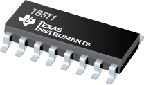
TB5T1
5V 双路全双工 PECL 收发器
The device is a dual differential driver/receiver circuit that transmits and receives digital data over balanced transmission lines. The dual drivers translate input TTL logic levels to differential pseudo-ECL output levels. The dual receivers convert differential-input logic levels to TTL output levels. Each driver or receiver pair has its own common enable control allowing serial data and a control clock to be transmitted and received on a single integrated circuit. The TB5T1 requires the customer to supply termination resistors on the circuit board.
The power-down loading characteristics of the receiver input circuit are approximately 8 k relative to the power supplies; hence, it does not load the transmission line when the circuit is powered down.
In circuits with termination resistors, the line remains impedance- matched when the circuit is powered down. The driver does not load the line when it is powered down.
All devices are characterized for operation from -40°C to 85°C.
The logic inputs of this device include internal pull-up resistors of approximately 40 k that are connected to VCC to ensure a logical high level input if the inputs are open circuited.
- .
- Functional Replacement for the Agere BTF1A
- .
- Driver Features
- .
- Third-State Logic Low Output
- .
- ESD Protection HBM > 3 kV, CDM > 2 kV
- .
- No Line Loading when VCC = 0
- .
- Capable of Driving 50- loads
- .
- 2.0-ns Maximum Propagation Delay
- .
- 0.2-ns Output Skew typical
- .
- Receiver Features
- .
- High-Input Impedance Approximately 8 k
- .
- 4.0-ns Maximum Propagation Delay
- .
- 50-mV Hysteresis
- .
- Slew Rate Limited 1 ns min 80% to 20%
- .
- ESD Protection HBM > 3 kV, CDM > 2 kV
- .
- -1.1-V to 7.1-V Input Voltage Range
- .
- Common Device Features
- .
- Common Enable for Each Driver/Receiver Pair
- .
- Operating Temperature Range: -40°C to 85°C
- .
- Single 5.0 V ± 10% Supply
- .
- Available in Gull-Wing SOIC JEDEC MS-013, DW and SOIC D Package

