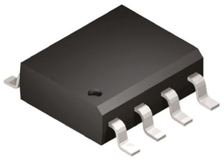
ADN4691EBRZ
ANALOG DEVICES ADN4691EBRZ 驱动器, LVDS, 半双工, LVDS 收发器, 130 ps, 24 mA, -40 °C, 85 °C, 3 V
Product Details
The ADN4691E/ADN4693E/ADN4696E/ADN4697E are multipoint, low voltage differential signaling M-LVDS transceivers driver and receiver pairs that can operate at up to 200 Mbps 100 MHz. The receivers detect the bus state with a differential input of as little as 50 mV over a common-mode voltage range of −1 V to +3.4 V. ESD protection of up to ±15 kV is implemented on the bus pins. The devices adhere to the TIA/EIA-899 standard for M-LVDS and complement TIA/EIA- 644 LVDS devices with additional multipoint capabilities.
The ADN4691E/ADN4693E are Type 1 receivers with 25 mV of hysteresis so that slow-changing signals or loss of input does not lead to output oscillations. The ADN4696E/ADN4697E are Type 2 receivers exhibiting an offset threshold, guaranteeing the output state when the bus is idle bus-idle fail-safe or the inputs are open open-circuit fail-safe.
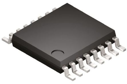
The devices are available as half-duplex in an 8-lead SOIC package the ADN4691E/ADN4696E or as full-duplex in a 14-lead SOIC package the ADN4693E/ADN4697E.
Applications
- .
- Backplane and cable multipoint data transmission
- .
- Multipoint clock distribution
- .
- Low power, high speed alternative to shorter RS-485 links
- .
- Networking and wireless base station infrastructure
### Features and Benefits
- .
- Multipoint LVDS transceivers low voltage differential signaling driver and receiver pairs
- .
- Switching rate: 200 Mbps 100 MHz
- .
- Supported bus loads: 30 Ω to 55 Ω
- .
- Type 1 receiver type: hysteresis of 25 mV
- .
- Conforms to TIA/EIA-899 standard for M-LVDS
- .
- Glitch free power-up/power-down on M-LVDS bus
- .
- Controlled transition times on driver output
- .
- Common-mode range: −1 V to +3.4 V, allowing communication with 2 V of ground noise
- .
- Driver outputs high-Z when disabled or powered off
- .
- See data sheet for additional features