TMS320VC5409APGE16
固定PointDigital信号处理器 Fixed-PointDigital Signal Processor
Introduction
This section lists the pin assignments and describes the function of each pin. This data manual also provides a detailed description section, electrical specifications, parameter measurement information, and mechanical data about the available packaging.
Description
The TMS320VC5409A fixed-point, digital signal processor DSP hereafter referred to as the 5409A unless otherwise specified is based on an advanced modified Harvard architecture that has one program memory bus and three data memory buses. This processor provides an arithmetic logic unit ALU with a high degree of parallelism, application-specific hardware logic, on-chip memory, and additional on-chip peripherals. The basis of the operational flexibility and speed of this DSP is a highly specialized instruction set.
TMS320VC5409A Features
• Advanced Multibus Architecture With Three Separate 16-Bit Data Memory Buses and One Program Memory Bus
• 40-Bit Arithmetic Logic Unit ALU Including a 40-Bit Barrel Shifter and Two Independent 40-Bit Accumulators
• 17- × 17-Bit Parallel Multiplier Coupled to a 40-Bit Dedicated Adder for Non-Pipelined Single-Cycle Multiply/Accumulate MAC Operation
• Compare, Select, and Store Unit CSSU for the Add/Compare Selection of the Viterbi Operator
• Exponent Encoder to Compute an Exponent Value of a 40-Bit Accumulator Value in a Single Cycle
• Two Address Generators With Eight Auxiliary Registers and Two Auxiliary Register Arithmetic Units ARAUs
• Data Bus With a Bus Holder Feature
• Extended Addressing Mode for 8M × 16-Bit Maximum Addressable External Program Space
• 32K × 16-Bit On-Chip RAM Composed of:
– Four Blocks of 8K × 16-Bit On-Chip Dual-Access Program/Data RAM
• 16K × 16-Bit On-Chip ROM Configured for Program Memory
• Enhanced External Parallel Interface XIO2
• Single-Instruction-Repeat and Block-Repeat Operations for Program Code
• Block-Memory-Move Instructions for Better Program and Data Management
• Instructions With a 32-Bit Long Word Operand
• Instructions With Two- or Three-Operand Reads
• Arithmetic Instructions With Parallel Store and Parallel Load
• Conditional Store Instructions
• Fast Return From Interrupt
• On-Chip Peripherals
– Software-Programmable Wait-State Generator and Programmable Bank-Switching
– On-Chip Programmable Phase-Locked Loop PLL Clock Generator With Internal Oscillator or External Clock Source1
– One 16-Bit Timer
– Six-Channel Direct Memory Access DMA Controller
– Three Multichannel Buffered Serial Ports McBSPs
– 8/16-Bit Enhanced Parallel Host-Port Interface HPI8/16
• Power Consumption Control With IDLE1, IDLE2, and IDLE3 Instructions With Power-Down Modes
• CLKOUT Off Control to Disable CLKOUT
• On-Chip Scan-Based Emulation Logic, IEEE Std 1149.1 JTAG Boundary Scan Logic 2
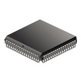
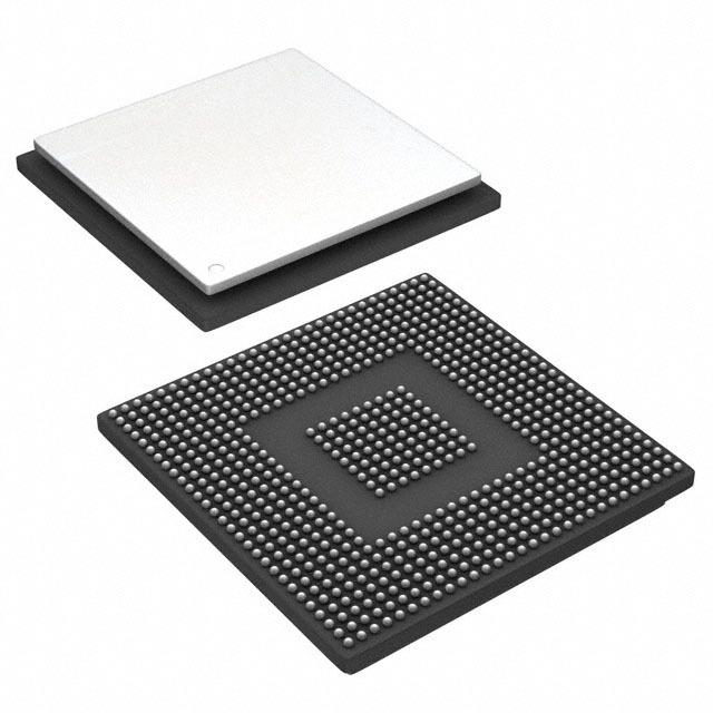
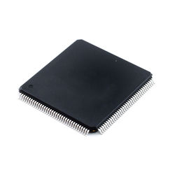
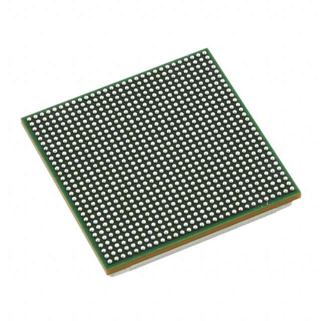
• 144-Pin Ball Grid Array BGA GGU Suffix
• 144-Pin Low-Profile Quad Flatpack LQFP PGE Suffix
• 6.25-ns Single-Cycle Fixed-Point Instruction Execution Time 160 MIPS
• 8.33-ns Single-Cycle Fixed-Point Instruction Execution Time 120 MIPS
• 3.3-V I/O Supply Voltage 160 and 120 MIPS
• 1.6-V Core Supply Voltage 160 MIPS
• 1.5-V Core Supply Voltage 120 MIPS