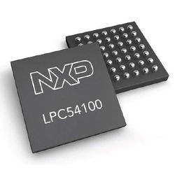
LPC54616J512BD100E
ARM MCU微控制单元, LPC Family LPC54000 Series Microcontrollers, ARM 皮质-M4, 32位, 180 MHz, 512 KB, 200 KB
Overview
The LPC546xx MCU family combines the power efficiency of the 220 MHz ARM® Cortex®-M4 core with multiple high-speed connectivity options, advanced timers, and analog features. DSP capabilities enable LPC546xx MCU devices to support complex algorithms in data-intensive application. Providing flexibility with up to 512 KB Flash and external memory interfaces, this family provides the ability to adapt as requirements change. Flash options support large, flexible internal and external memory configurations. Compatibility within the LPC54000 series enables the LPC546xx MCU family to provide a seamless migration path for increasing processing power and adding the flexibility of additional advanced peripherals.
MoreLess
## Features
### ARM Cortex-M4 core version r0p1
* ARM Cortex-M4 processor, running at a frequency of up to 180 MHz.
* Floating Point Unit FPU and Memory Protection Unit MPU.
* ARM Cortex-M4 built-in Nested Vectored Interrupt Controller NVIC.
* Non-maskable Interrupt NMI input with a selection of sources.
* Serial Wire Debug SWD with six instruction breakpoints, two literal comparators, and four watch points. Includes Serial Wire Output and ETM Trace for enhanced debug capabilities, and a debug timestamp counter.
* System tick timer.
### On-chip memory
* Up to 512 KB on-chip flash program memory with flash accelerator and 256 byte page erase and write.
* Up to 200 KB total SRAM consisting of 160 KB contiguous main SRAM and an additional 32 KB SRAM on the I&D buses. 8 KB of SRAM bank intended for USB traffic.
* 16 KB of EEPROM.
### ROM API support
* Flash In-Application Programming IAP and In-System Programming ISP.
* ROM-based USB drivers HID, CDC, MSC, and DFU. Flash updates via USB.
* Booting from valid user code in flash, USART, SPI, and I2C.
* Legacy, Single, and Dual image boot.
* OTP API for programming OTP memory.
* Random Number Generator RNG API.
### Serial interfaces
* Flexcomm Interface contains ten serial peripherals. Each Flexcomm Interface can be selected by software to be a USART, SPI, or I2C interface. Two Flexcomm Interfaces also include an I2S interface. Each Flexcomm Interface includes a FIFO that supports USART, SPI, and I2S if supported by that Flexcomm Interface. A variety of clocking options are available to each Flexcomm Interface and include a shared fractional baud-rate generator.
* I2C-bus interfaces support Fast-mode and Fast-mode Plus with data rates of up to 1Mbit/s and with multiple address recognition and monitor mode. Two sets of true I2C pads also support High Speed Mode 3.4 Mbit/s as a slave.
* Two ISO 7816 Smart Card Interfaces with DMA support.
* USB 2.0 high-speed host/device controller with on-chip high-speed PHY.
* USB 2.0 full-speed host/device controller with on-chip PHY and dedicated DMA controller supporting crystal-less operation in device mode.
* SPIFI with XIP feature uses up to four data lines to access off-chip SPI/DSPI/QSPI flash memory at a much higher rate than standard SPI or SSP interfaces.
* Ethernet MAC with MII/RMII interface with Audio Video Bridging AVB support and dedicated DMA controller.
* Two CAN FD modules with dedicated DMA controller.
### Digital peripherals
* DMA controller with 30 channels and up to 24 programmable triggers, able to access all memories and DMA-capable peripherals.
* LCD Controller supporting both Super-Twisted Nematic STN and Thin-Film Transistor TFT displays. It has a dedicated DMA controller, selectable display resolution up to 1024 x 768 pixels, and supports up to 24-bit true-color mode.
* External Memory Controller EMC provides support for asynchronous static memory devices such as RAM, ROM and flash, in addition to dynamic memories such as single data rate SDRAM with an SDRAM clock of up to 100 MHz.
* Secured digital input/output SD/MMC and SDIO card interface with DMA support.
* CRC engine block can calculate a CRC on supplied data using one of three standard polynomials with DMA support.
* Up to 171 General-Purpose Input/Output GPIO pins.
* GPIO registers are located on the AHB for fast access. The DMA supports GPIO ports.
* Up to eight GPIOs can be selected as Pin Interrupts PINT, triggered by rising, falling or both input edges.
* Two GPIO Grouped Interrupts GINT enable an interrupt based on a logical AND/OR combination of input states.
* CRC engine.
### Analog peripherals
* 12-bit ADC with 12 input channels and with multiple internal and external trigger inputs and sample rates of up to 5.0 MSamples/sec. The ADC supports two independent conversion sequences.
* Integrated temperature sensor connected to the ADC.
### Timers
* Five 32-bit general purpose timers/counters, four of which support up to four capture inputs and four compare outputs, PWM mode, and external count input. Specific timer events can be selected to generate DMA requests. The fifth timer does not have external pin connections and may be used for internal timing operations.
* One SCTimer/PWM with eight input and ten output functions including capture and match. Inputs and outputs can be routed to or from external pins and internally to or from selected peripherals. Internally, the SCTimer/PWM supports 16 match/captures, 16 events, and 16 states.
* 32-bit Real-time clock RTC with 1 s resolution running in the always-on power domain. A timer in the RTC can be used for wake-up from all low power modes including deep power-down, with 1 ms resolution.
* Multiple-channel multi-rate 24-bit timer MRT for repetitive interrupt generation at up to four programmable, fixed rates.
* Windowed Watchdog Timer WWDT.
* Repetitive Interrupt Timer RIT for debug time stamping and for general purpose use.
### Security peripherals
* Enhanced Code Read Protection eCRP to protect user code.
### Clock generation
* 12 MHz internal Free Running Oscillator FRO. This oscillator provides a selectable 48 MHz or 96 MHz output, and a 12 MHz output divided down from the selected higher frequency that can be used as a system clock. The FRO is trimmed to ±1 % accuracy over the entire voltage and temperature range.
* External clock input for clock frequencies of up to 25 MHz.
* Crystal oscillator with an operating range of 1 MHz to 25 MHz.
* Watchdog Oscillator WDTOSC with a frequency range of 6 kHz to 1.5 MHz.
* 32.768 kHz low-power RTC oscillator.
* System PLL allows CPU operation up to the maximum CPU rate and can run from the main oscillator, the internal FRO, the watchdog oscillator or the 32.768 KHz RTC oscillator.
* Two additional PLLs for USB clock and audio subsystem.
* Independent clocks for the SPIFI interface, ADC, USBs, and the audio subsystem.
* Clock output function with divider.
* Frequency measurement unit for measuring the frequency of any on-chip or off-chip clock signal.
### Additional information
* DMIC subsystem including a dual-channel PDM microphone interface, flexible decimators, 16 entry FIFOs, optional DC locking, hardware voice activity detection, and the option to stream the processed output data to I2S.
* Single power supply 1.71 V to 3.6 V.
* Power-On Reset POR.
* Brown-Out Detect BOD with separate thresholds for interrupt and forced reset.
* JTAG boundary scan supported.
* 128 bit unique device serial number for identification.
* Operating temperature range -40 °C to +105 °C.


