AD650BD
电压 - 频率和频率 - 电压转换器 Voltage-to-Frequency and Frequency-to-Voltage Converter
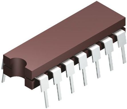
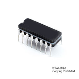
电压到频率和频率到电压 转换器 IC ±0.1% 14-CDIP
得捷:
IC F/V & V/F CONV 1MHZ 14CDIP
贸泽:
电压频率转换及频率电压转换 IC V/F CONVERTER
艾睿:
The AD650BD V2F and F2V from Analog Devices can provide you with greater resources for your processor s normal operations. Its typical dual supply voltage is ±12|±15 V, with a minimum of ±9 V and maximum of ±18 V. This part has a temperature range of -25 °C to 85 °C. This device comes in tube packaging. This device uses dual power supplies.
Jameco:
VFC-FVC Non Sync 1 MHz 14-Pin SBC DIP
安富利:
The AD650 V/F/V voltage-to-frequency or frequency-to-voltage converter provides a combination of high frequency operation and low nonlinearity previously unavailable in monolithic form. The inherent monotonicity of the V/F transfer function makes the AD650 useful as a high-resolution analog-to-digital converter. A flexible input configuration allows a wide variety of input voltage and current formats to be used, and an open-collector output with separate digital ground allows simple interfacing to either standard logic families or opto-couplers. The linearity error of the AD650 is typically 20 ppm 0.002% of full scale and 50 ppm 0.005% maximum at 10 kHz full scale. This corresponds to approximately 14-bit linearity in an analogto-digital converter circuit. Higher full-scale frequencies or longer count intervals can be used for higher resolution conversions. The AD650 has a useful dynamic range of six decades allowing extremely high resolution measurements. Even at 1 MHz full scale, linearity is guaranteed less than 1000 ppm 0.1% on the AD650KN, BD, and SD grades. In addition to analog-to-digital conversion, the AD650 can be used in isolated analog signal transmission applications, phased-locked loop circuits, and precision stepper motor speed controllers. In the F/V mode, the AD650 can be used in precision tachometer and FM demodulator circuits. The input signal range and full-scale output frequency are userprogrammable with two external capacitors and one resistor. Input offset voltage can be trimmed to zero with an external potentiometer. The AD650JN and AD650KN are offered in plastic 14-lead DIP packages. The AD650JP is available in a 20-lead plastic leaded chip carrier PLCC. Both plastic packaged versions of the AD650 are specified for the commercial temperature range 0°C to 70°C. For industrial temperature range −25°C to +85°C applications, the AD650AD and AD650BD are offered in ceramic packages. The AD650SD is specified for the full −55°C to +125°C extended temperature range.
Chip1Stop:
VFC/FVC Non-Sync 1MHz 14-Pin SBCDIP Tube
Verical:
VFC/FVC Non-Sync 1MHz 14-Pin SBCDIP Tube
罗切斯特:
Voltage to Frequency Converter, 1 Func, 1MHz, Bipolar, CDIP14