DK-START-4CGX15N/P
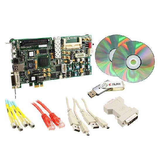
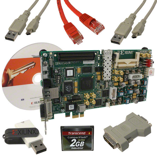
Cyclone IV GX Transceiver Starter Kit, AlteraAltera"s Cyclone® IV GX Transceiver Starter Kit provides a low-cost platform for developing transceiver I/O-based FPGA designs. This kit includes the complete hardware and software for you to: Develop your FPGA design for cost-sensitive applications, measure the FPGA"s low power consumption, test signal quality of the FPGA transceiver I/Os up to 2.5Gbps develop and test PCI Express® 1.0 endpoint x1 lane designs ∼250Mbps transfer rate.Cyclone IV GX EP4CGX15BF14C8N FPGA MAX® II CPLD EPM2210 System Controller enabling passive serial PS configuration from Flash Embedded USB-Blaster™ for using the Quartus II Programmer JTAG header for external USB-Blaster Altera EPCS serial configuration device FPGA clock sources: 50MHz, 125MHz, and SMA clock input Other on-board oscillators: 6MHz, 24MHz, and 25MHz LEDs Two-line character LCD display Push-buttons 16MB of Flash memory 2MB of synchronous SRAM PCI Express edge connector 10/100/1000BASE-T Ethernet PHY with RJ-45 connector or one transceiver to SMA connectors requires a minor board modification On-board power measurement circuitry Laptop DC power input PCI Express edge power connector Power regulators: LT3027 and LT3023 Step-down switching regulator: LT3510 ADC: LTC2418 PCI Express low-profile 6.6 x 2.713in board form factor ### 注CDs/DVDs are no longer included in Altera development kits. All development kit content can be downloaded from the Altera web site.### 现场可编程门阵列 FPGAFPGA 是一种半导体设备,包含通过可编程互连连接的可配置逻辑块 CLB 矩阵。 用户通过编程 SRAM 确定这些互连。 CLB 可以简单(与或门等),也可以复杂(RAM 块)。 FPGA 允许对设计进行更改,即使在设备焊接到印刷电路板上之后。
Cyclone IV GX Transceiver Starter Kit,
Altera"s Cyclone® IV GX Transceiver Starter Kit provides a low-cost platform for developing transceiver I/O-based FPGA designs. This kit includes the complete hardware and software for you to: Develop your FPGA design for cost-sensitive applications, measure the FPGA"s low power consumption, test signal quality of the FPGA transceiver I/Os up to 2.5Gbps develop and test PCI Express® 1.0 endpoint x1 lane designs ∼250Mbps transfer rate.
Cyclone IV GX EP4CGX15BF14C8N FPGA
MAX® II CPLD EPM2210 System Controller enabling passive serial PS configuration from Flash
Embedded USB-Blaster™ for using the Quartus II Programmer
JTAG header for external USB-Blaster
Altera EPCS serial configuration device
FPGA clock sources: 50MHz, 125MHz, and SMA clock input
Other on-board oscillators: 6MHz, 24MHz, and 25MHz
LEDs
Two-line character LCD display
Push-buttons
16MB of Flash memory
2MB of synchronous SRAM
PCI Express edge connector
10/100/1000BASE-T Ethernet PHY with RJ-45 connector or one transceiver to SMA connectors requires a minor board modification
On-board power measurement circuitry
Laptop DC power input
PCI Express edge power connector
Power regulators: LT3027 and LT3023
Step-down switching regulator: LT3510
ADC: LTC2418
PCI Express low-profile 6.6 x 2.713in board form factor
### 注
CDs/DVDs are no longer included in Altera development kits. All development kit content can be downloaded from the Altera web site.
FPGA 是一种半导体设备,包含通过可编程互连连接的可配置逻辑块 CLB 矩阵。 用户通过编程 SRAM 确定这些互连。 CLB 可以简单(与或门等),也可以复杂(RAM 块)。 FPGA 允许对设计进行更改,即使在设备焊接到印刷电路板上之后。