ADL5570
2.3 GHz至2.4 GHz的WiMAX的功率放大器 2.3 GHz to 2.4 GHz WiMAX Power Amplifier
Product Details
The is a high linearity 2.3 GHz to 2.4 GHz power amplifier designed for WiMAX terminals using TDD operation at a duty cycle of 31%. With a gain of 29 dB and an output compression point of 31 dBm at 2.35 GHz, it can operate at an output power level up to 26 dBm while maintaining an EVM of ≤3% OFDM 16 or 64 QAM with a supply voltage of 3.5 V. PAE is 20% @ POUT = 25 dBm.
The ADL5570 RF input is matched on-chip and provides an input return loss of less than −10 dB. The open-collector output is externally matched with strip-line and external shunt capacitance.
The ADL5570 operates over a supply voltage range from 3.2 V to 4.2 V with a supply current of 440 mA burst rms when delivering 25 dBm 3.5 V supply. A low power mode is also available for operation at power levels of ≤10 dBm with optimized operating and quiescent currents of 100 mA and 70 mA, respectively. A standby mode is available that reduces the quiescent current to 1 mA, which is useful when a TDD terminal is receiving data.
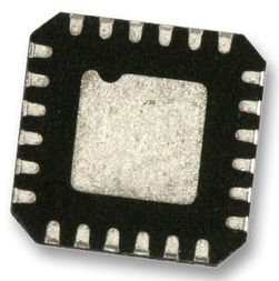
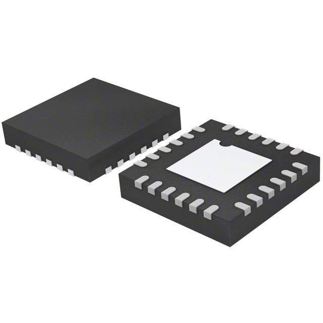
The ADL5570 is fabricated in a GaAs HBT process and is packaged in a 4 mm × 4 mm, 16-lead, Pb-free RoHS-compliant LFCSP that uses an exposed paddle for excellent thermal impedance. It operates from −40°C to +85°C.
**Applications**
* WiMAX/WiBro mobile terminals
Data Sheet, Rev. 0, 6/07
### Features and Benefits
- .
- Fixed gain of 29 dB
- .
- Operation from 2.3 GHz to 2.4 GHz
- .
- EVM ≤ 3% at POUT = 25 dBm with 16 QAM OFDMA
- .
- Quiescent current
130 mA in high power mode
70 mA in low power mode
- .
- Input internally matched to 50 Ω
- .
- Power supply: 3.2 V to 4.2 V
- .
- Power-added efficiency PAE: 20%
- .
- Multiple operating modes to reduce battery drain
Low power mode: 100 mA
Standby mode: 1mA
Sleep mode: <1 μA