OPA4872-EP
增强型产品 4:1 高速多路复用器
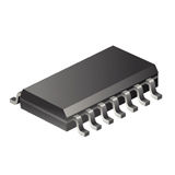
The OPA4872 offers a very wideband 4:1 multiplexer in an SO-14 package. Using only 10.6 mA, the OPA4872 provides a user-settable output amplifier gain with greater than 500-MHz large-signal bandwidth 2 VPP. The switching glitch is improved over earlier solutions using a new patented input stage switching approach. This technique uses current steering as the input switch while maintaining an overall closed-loop design. The OPA4872 exhibits an off isolation of 88dB in either Disable or Shutdown mode. With greater than 500-MHz small-signal bandwidth at a gain of 2, the OPA4872 gives a typical 0.1-dB gain flatness to greater than 120 MHz.
System power may be optimized using the chip-enable feature for the OPA4872. Taking the chip enable EN line high powers down the OPA4872 to less than 3.4 mA total supply current. Further power reduction to 1.1mA quiescent current can be achieved by bringing the shutdown SD line high. Muxing multiple OPA4872s outputs together, then using the chip enable to select which channels are active, increases the number of possible inputs.
- .
- 500-MHz Small-Signal Bandwidth
- .
- 500-MHz, 2-VPP Bandwidth
- .
- 0.1-dB Gain Flatness to 120 MHz
- .
- 10-ns Channel-Switching Time
- .
- Low Switching Glitch: 40 mVPP
- .
- 2300-V/µs Slew Rate
- .
- 0.035%/0.005° Differential Gain, Phase
- .
- Quiescent Current = 10.6 mA
- .
- 1.1-mA Quiescent Current in Shutdown Mode
- .
- 88-dB Off Isolation in Disable or Shutdown
10 MHz
- .
- APPLICA ONS
- .
- Video Router
- .
- LCD and Plasma Display
- .
- High Speed PGA
- .
- Drop-In Upgrade to AD8174
- .
- SUPPORTS DEFENSE, AEROSPACE, AND MEDICAL APPLICATIONS
- .
- Controlled Baseline
- .
- One Assembly/Test Site
- .
- One Fabrication Site
- .
- Available in Military 55°C/125°C, Temperature Range1
- .
- Extended Product Life Cycle
- .
- Extended Product-Change Notification
- .
- Product Traceability
1 Additional temperature ranges available - contact factory
All other trademarks are the property of their respective owners.


