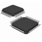
ADUC7029BBCZ62
ANALOG DEVICES ADUC7029BBCZ62 微控制器, 32位, 精准模拟, ARM7TDMI, 41.78 MHz, 62 KB, 8 KB, 49 引脚, BGA
Product Details
The ADuC7019/ADuC7020/ADuC7021/ADuC7022/ADuC7024/ADuC7025/ ADuC7026/ADuC7027/ADuC7028/ADuC7029 are fully integrated, 1 MSPS, 12-bit data acquisition systems incorporating high performance multichannel ADCs, 16-bit/32-bit MCUs, and Flash®/EE memory on a single chip.
The ADC consists of up to 12 single-ended inputs. An additional four inputs are available but are multiplexed with the four DAC output pins. The four DAC outputs are available only on certain models ADuC7020, ADuC7026, ADuC7028, and ADuC7029. However, in many cases where the DAC outputs are not present, these pins can still be used as additional ADC inputs, giving a maximum of 16 ADC input channels. The ADC can operate in single-ended or differential input mode. The ADC input voltage is 0 V to VREF. A low drift band gap reference, temperature sensor, and voltage comparator complete the ADC peripheral set.
Depending on the part model, up to four buffered voltage output DACs are available on-chip. The DAC output range is programmable to one of three voltage ranges.
The devices operate from an on-chip oscillator and a PLL generating an internal high frequency clock of 41.78 MHz UCLK. This clock is routed through a programmable clock divider from which the MCU core clock operating frequency is generated. The microcontroller core is an ARM7TDMI®, 16-bit/32-bit RISC machine, which offers up to 41 MIPS peak performance. Eight kilobytes of SRAM and 62 kilobytes of nonvolatile Flash/EE memory are provided on-chip. The ARM7TDMI core views all memory and registers as a single linear array.
On-chip factory firmware supports in-circuit serial download via the UART or I2 C serial interface port; nonintrusive emulation is also supported via the JTAG interface. These features are incorporated into a low cost QuickStart™ development system supporting this MicroConverter® family.
The parts operate from 2.7 V to 3.6 V and are specified over an industrial temperature range of −40°C to +125°C. When operating at 41.78 MHz, the power dissipation is typically 120 mW. The ADuC7019/ADuC7020/ADuC7021/ ADuC7022/ADuC7024/ADuC7025/ADuC7026/ADuC7027/ADuC7028/ ADuC7029 are available in a variety of memory models and packages see Ordering Guide.
Applications
- .
- Industrial control and automation systems
- .
- Smart sensors, precision instrumentation
- .
- Base station systems, optical networking
### Features and Benefits
- .
- Analog I/O
- .
- Multichannel, 12-bit, 1 MSPS ADC
Up to 16 ADC channels
- .
- Fully differential and single-ended modes
- .
- 0 V to VREF analog input range
- .
- 12-bit voltage output DACs
Up to 4 DAC outputs available
- .
- On-chip voltage reference
- .
- On-chip temperature sensor ±3°C
- .
- Voltage comparator
- .
- Microcontroller
- .
- ARM7TDMI core, 16-bit/
32-bit RISC architecture
- .
- JTAG port supports code download and debug
- .
- Clocking options
- .
- Trimmed on-chip oscillator ±3%
- .
- External watch crystal
- .
- External clock source up to 44 MHz
- .
- 41.78 MHz PLL with programmable divider
- .
- Refer to data sheet for additional features.