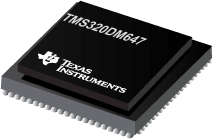
TMS320DM647
数字媒体处理器 Digital Media Processor
The TMS320C64x+™ DSPs including the /TMS320DM648 devices are the highest-performance fixed-point DSP generation in the TMS320C6000™ DSP platform. The DM647, DM648 devices are based on the third-generation high-performance, advanced Veloci™ very-long-instruction-word VLIW architecture developed by Texas Instruments TI, making these DSPs an excellent choice for digital media applications. The C64x+™ devices are upward code-compatible from previous devices that are part of the C6000™ DSP platform. The C64x™ DSPs support added functionality and have an expanded instruction set from previous devices.
Any reference to the C64x DSP or C64x CPU also applies, unless otherwise noted, to the C64x+ DSP and C64x+ CPU, respectively.
With performance of up to 8800 million instructions per second MIPS at a clock rate of 1.1 GHz, the C64x+ core offers solutions to high-performance DSP programming challenges. The DSP core possesses the operational flexibility of high-speed controllers and the numerical capability of array processors. The C64x+ DSP core processor has 64 general-purpose registers of 32-bit word length and eight highly independent functional units—two multipliers for a 32-bit result and six arithmetic logic units ALUs. The eight functional units include instructions to accelerate the performance in video and imaging applications. The DSP core can produce four 16-bit multiply-accumulates MACs per cycle for up to 4400 million MACs per second MMACS, or eight 8-bit MACs per cycle for up tp 8800 MMACS. For more details on the C64x+ DSP, see the literature number SPRU732.
The devices also have application-specific hardware logic, on-chip memory, and additional on-chip peripherals similar to the other C6000 DSP platform devices. The core uses a two-level cache-based architecture. The Level 1 program cache L1P is a 256K-bit direct mapped cache and the Level 1 data cache L1D is a 256K-bit 2-way set-associative cache. The Level 2 memory/cache L2 consists of a 4M-bit DM648 or 2M-bit DM647 memory space that is shared between program and data space. L2 memory can be configured as mapped memory, cache, or combinations of the two.
The peripheral set includes five configurable 16-bit video port peripherals VP0, VP1, VP2, VP3, and VP4. These video port peripherals provide a glueless interface to common video decoder and encoder devices. The video port peripherals support multiple resolutions and video standards e.g., CCIR601, ITU-BT.656, BT.1120, SMPTE 125M, 260M, 274M, and 296M, a VCXO interpolated control port VIC; a 1000 Mbps Ethernet Switch Subsystem with a management data input/output MDIO module and two SGMII ports DM648 or one SGMII port only DM647; a 4-bit transmit, 4-bit receive VLYNQ interface; an inter-integrated circuit I2C bus interface; a multichannel audio serial port McASP with ten serializers; four 64-bit general-purpose timers each configurable as two independent 32-bit timers; a user-configurable 16-bit or 32-bit host-port interface HPI; 32 pins for general-purpose input/output GPIO with programmable interrupt/event generation modes, multiplexed with other peripherals; one UART; and two glueless external memory interfaces: a synchronous and asynchronous external memory interface EMIFA for slower memories/peripherals, and a higher DDR2 SDRAM interface.
The video port peripherals provide a glueless interface to common video decoder and encoder devices. The video port peripherals support multiple resolutions and video standards e.g., CCIR601, ITU-BT.656, BT.1120, SMPTE 125M, 260M, 274M, and 296M.
The video port peripherals are configurable and can support either video capture and/or video display modes. Each video port consists of two channels A and B with a 5120-byte capture/display buffer that is splittable between the two channels.
For more details on the video port peripherals, see the literature number SPRUEM1.
The management data input/output MDIO module continuously polls all 32 MDIO addresses to enumerate all PHY devices in the system.
The I2C and VLYNQ ports allow the device to easily control peripheral modules and/or communicate with host processors.
The rich peripheral set provides the ability to control external peripheral devices and communicate with external processors. For details on each of the peripherals, see the related sections later in this document and the associated peripheral reference guides.
The devices have a complete set of development tools. These include C compilers, a DSP assembly optimizer to simplify programming and scheduling, and a Windows™ debugger interface for visibility into source code execution.
- .
- High-Performance Digital Media Processor
- .
- 720-MHz, 800-MHz, 900-MHz, 1.1-GHz C64x+™ Clock Rates
- .
- 1.39 ns -720, 1.25 ns -800, 1.11 ns -900, 0.91 ns -1100 Instruction Cycle Time
- .
- 5760, 6400, 7200, 8800 MIPS
- .
- Eight 32-Bit C64x+ Instructions/Cycle
- .
- Fully Software-Compatible With C64x/Debug
- .
- Commercial Temperature Ranges -720, -900, and -1100 only
- .
- Extended Temperature Ranges -800 only
- .
- Industrial Temperature Ranges -720, -900, and -1100 only
- .
- VelociTI.2™ Extensions to VelociTI™
Advanced Very-Long-Instruction-Word VLIW TMS320C64x+™ DSP Core
- .
- Eight Highly Independent Functional Units With VelociTI.2 Extensions:
- .
- Six ALUs 32-/40-Bit, Each Supports Single 32-bit, Dual 16-bit, or Quad 8-bit Arithmetic per Clock Cycle
- .
- Two Multipliers Support Four 16 x 16-bit Multiplies 32-bit Results per Clock Cycle or Eight 8 x 8-bit Multiplies 16-Bit Results per Clock Cycle
- .
- Load-Store Architecture With Non-Aligned Support
- .
- 64 32-bit General-Purpose Registers
- .
- Instruction Packing Reduces Code Size
- .
- All Instructions Conditional
- .
- Additional C64x+™ Enhancements
- .
- Protected Mode Operation
- .
- Exceptions Support for Error Detection and Program Redirection
- .
- Hardware Support for Modulo Loop Auto-Focus Module Operation
- .
- C64x+ Instruction Set Features
- .
- Byte-Addressable 8-/16-/32-/64-bit Data
- .
- 8-bit Overflow Protection
- .
- Bit-Field Extract, Set, Clear
- .
- Normalization, Saturation, Bit-Counting
- .
- VelociTI.2 Increased Orthogonality
- .
- C64x+ Extensions
- .
- Compact 16-bit Instructions
- .
- Additional Instructions to Support Complex Multiplies
- .
- C64x+ L1/L2 Memory Architecture
- .
- 256K-bit 32K-byte L1P Program RAM/Cache [Direct Mapped]
- .
- 256K-bit 32K-byte L1D Data RAM/Cache
[2-Way Set-Associative]
- .
- 2M-bit/256K-byte DM647 or 4M-Bit/512K-byte DM648 L2 Unified Mapped RAM/Cache [Flexible Allocation]
- .
- Supports Little Endian Mode Only
- .
- Five Configurable Video Ports
- .
- Providing a Glueless I/F to Common Video Decoder and Encoder Devices
- .
- Supports Multiple Resolutions/Video Standards
- .
- VCXO Interpolated Control Port VIC
- .
- Supports Audio/Video Synchronization
- .
- External Memory Interfaces EMIFs
- .
- 32-Bit DDR2 SDRAM Memory Controller With 512M-Byte Address Space 1.8-V I/O
- .
- Asynchronous 16-Bit Wide EMIF EMIFA
- .
- Up to 128M-Byte Total Address Reach
- .
- 64M-Byte Address Reach per CE Space
- .
- Glueless Interface to Asynchronous Memories SRAM, Flash, and EEPROM
- .
- Synchronous Memories SBSRAM and ZBT SRAM
- .
- Supports Interface to Standard Sync Devices and Custom Logic FPGA, CPLD, ASICs, etc.
- .
- Enhanced Direct-Memory-Access EDMA Controller 64 Independent Channels
- .
- 3-Port Gigabit Ethernet Switch Subsystem
- .
- Four 64-Bit General-Purpose Timers Each Configurable as Two 32-Bit Timers
- .
- One UART With RTS and CTS Flow Control
- .
- One 4-wire Serial Port Interface SPI With Two Chip-Selects
- .
- Master/Slave Inter-Integrated Circuit I2C Bus™
- .
- Multichannel Audio Serial Port McASP
- .
- Ten Serializers and SPDIF DIT Mode
- .
- 16/32-Bit Host-Port Interface HPI
- .
- Advanced Event Triggering AET Compatible
- .
- 32-Bit 33-/66-MHz, 3.3-V Peripheral Component Interconnect PCI Master/Slave Interface Conforms to PCI Specification 2.3
- .
- VLYNQ™ Interface FPGA Interface
- .
- On-Chip ROM Bootloader
- .
- Individual Power-Saving Modes
- .
- Flexible PLL Clock Generators
- .
- IEEE-1149.1 JTAG™ Boundary-Scan-Compatible
- .
- 32 General-Purpose I/O GPIO Pins Multiplexed With Other Device Functions
- .
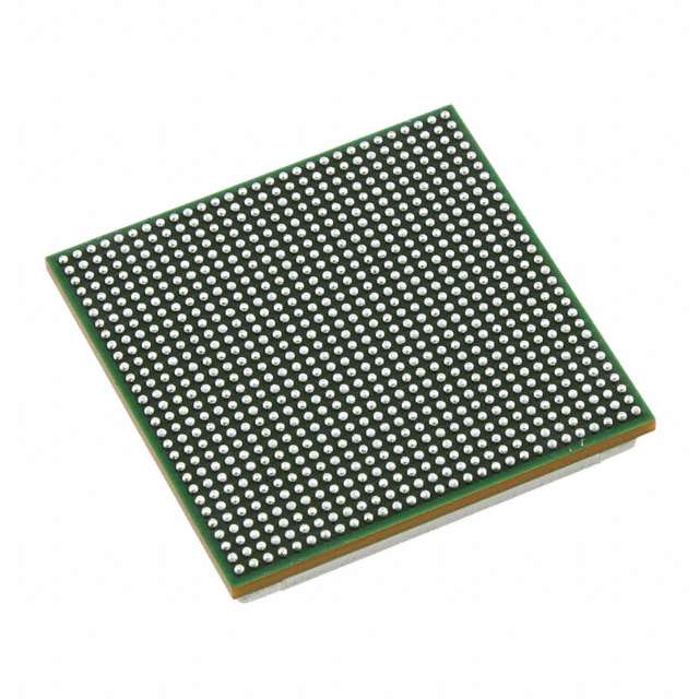
- Package:
- .
- 529-pin nFBGA ZUT suffix
- .
- 19x19 mm 0.8 mm pitch BGA
- .
- 0.09-µm/6-Level Cu Metal Process CMOS
- .
- 3.3-V and 1.8-V I/O, 1.2-V Internal -720, -800, -900, -1100