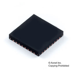
AD9144BCPAZRL
Digital to Analog Converters - DAC 16Bit 2.8GSPS Quad DAC 10Gbps JESD204B
Product Details
The AD9144 is a quad, 16-bit, high dynamic range digital-to-analog converter DAC that provides a maximum sample rate of 2.8 GSPS, permitting a multicarrier generation up to the Nyquist frequency. The DAC outputs are optimized to interface seamlessly with the ADRF6720 analog quadrature modulator AQM from Analog Devices, Inc. An optional 3-wire or 4-wire serial port interface SPI provides for programming/readback of many internal parameters. Full-scale output current can be programmed over a typical range of 13.9 mA to 27.0 mA. The AD9144 is available in an 88-lead LFCSP.
Product Highlights
1. Greater than 1 GHz, ultrawide complex signal bandwidth enables emerging wideband and multiband wireless applications.
2. Advanced low spurious and distortion design techniques provide high quality synthesis of wideband signals from baseband to high intermediate frequencies.
3. JESD204B Subclass 1 support simplifies multichip synchronization in software and hardware design.
4. Fewer pins for data interface width with serializer/ deserializer SERDES JESD204B eight-lane interface.
5. Programmable transmit enable function allows easy design balance between power consumption and wake-up time.
6. Small package size with 12 mm × 12 mm footprint.
Applications
- .
- Wireless communications
3G/4G W-CDMA base stations
Wideband repeaters
Software defined radios
- .
- Wideband communications
Point-to-point
Local multipoint distribution service LMDS and multichannel multipoint distribution service MMDS
- .
- Transmit diversity, multiple input/multiple output MIMO
- .
- Instrumentation
- .
- Automated test equipment
### Features and Benefits
- .
- Supports input data rate >1 GSPS
- .
- Proprietary low spurious and distortion design
6-carrier GSM IMD = 77 dBc at 75 MHz IF
SFDR = 82 dBc at DC IF, -9dBFS
Flexible 8-lane JESD204B interface
Support dual DAC mode at 2.8GSPS
- .
- Multiple chip synchronization
Fixed latency
Data generator latency compensation
- .
- Selectable 1×, 2×, 4×, 8× interpolation filter
Low power architecture
- .
- Input signal power detection
Emergency stop for downstream analog circuitry protection
- .
- Transmit enable function allows extra power saving
- .
- High performance, low noise PLL clock multiplier
- .
- Digital inverse sinc filter
- .
- Low power: 1.6 W at 1.6 GSPS, 1.7 W at 2.0 GSPS, full operating conditions
- .
- 88-lead LFCSP with exposed pad