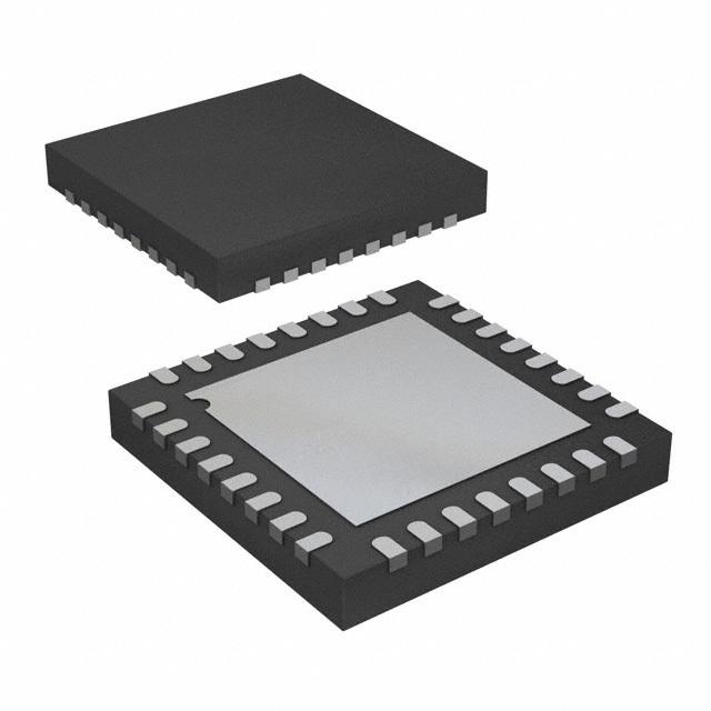
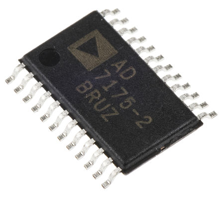
AD7172-4BCPZ-RL7
ADC Single Delta-Sigma 31.25KSPS 24Bit Serial 32Pin LFCSP T/R
Product Details
The AD7172-4 is a low noise, low power, multiplexed, Σ-Δ analog-to-digital converter ADC with 4- or 8-channel fully differential/single-ended inputs for low bandwidth signals. The AD7172-4 has a maximum channel scan rate of 6.21 kSPS 161 μs for fully settled data. The output data rates range from 1.25 SPS to 31.25 kSPS.
The AD7172-4 integrates key analog and digital signal conditioning blocks to allow users to configure an individual setup for each analog input channel in use via the SPI. Integrated true rail-to-rail buffers on the analog inputs and reference inputs provide easy to drive high impedance inputs.
The digital filter allows simultaneous 50 Hz and 60 Hz rejection at a 27.27 SPS output data rate. The user can switch between different filter options according to the demands of each channel in the application, with further digital processing functions such as offset and gain calibration registers, which are configurable on a per channel basis. General-purpose input/outputs GPIOs control external multiplexers synchronous to the ADC conversion timing. The specified temperature range is −40°C to +105°C.
The AD7172-4 is in a 5 mm × 5 mm, 32-lead LFCSP.
Note that, throughout this data sheet, the dual function pin names are referenced by the relevant function only.
Applications
- .
- Process control: PLC/DCS modules
- .
- Temperature and pressure measurement
- .
- Medical and scientific multichannel instrumentation
- .
- Chromatography
### Features and Benefits
- .
- Fast and flexible output rate: 1.25 SPS to 31.25 kSPS
- .
- Channel scan data rate of 6.21 kSPS/channel 161 μs settling
- .
- Performance specifications
- .
- 17.2 noise free bits at 31.25 kSPS
- .
- 24 noise free bits at 5 SPS
- .
- INL: ±2 ppm of FSR
- .
- 85 dB rejection of 50 Hz and 60 Hz with 50 ms settling
- .
- User configurable input channels
- .
- 4 fully differential channels or 8 single-ended channels
- .
- Crosspoint multiplexer
- .
- True rail-to-rail analog and reference input buffers
- .
- Internal or external clock
- .
- Power supply
- .
- AVDD1 = 3.0 V to 5.5 V, AVDD2 = IOVDD = 2 V to 5.5 V
- .
- Split supply with AVDD1 and AVSS at ±2.5 V or ±1.65 V
- .
- ADC current: 1.5 mA
- .
- Temperature range: −40°C to +105°C
- .
- 3- or 4-wire serial digital interface Schmitt trigger on SCLK
- .
- Serial port interface SPI, QSPI-, MICROWIRE-, and DSPcompatible