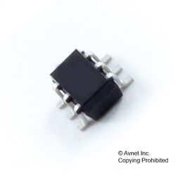
AD5611BKSZ-500RL7
ANALOG DEVICES AD5611BKSZ-500RL7 数模转换器, 10 bit, 串行, 2.7V 至 5.5V, SC-70, 6 引脚
Product Details
The AD5601/AD5611/AD5621, members of the _nano_DAC® family, are single, 8-/10-/12-bit, buffered voltage output DACs that operate from a single 2.7 V to 5.5 V supply, consuming typically 75 μA at 5 V. The parts come in a tiny LFCSP and SC70 packages. Their on-chip precision output amplifier allows rail-to-rail output swing to be achieved. The AD5601/AD5611/AD5621 utilize a versatile 3-wire serial interface that operates at clock rates up to 30 MHz and is compatible with SPI, QSPI™, MICROWIRE™, and DSP interface standards.
The reference for the AD5601/AD5611/AD5621 is derived from the power supply inputs and, therefore, gives the widest dynamic output range. The parts incorporate a power-on reset circuit, which ensures that the DAC output powers up to 0 V and remains there until a valid write to the device takes place.
The AD5601/AD5611/AD5621 contain a power-down feature that reduces current consumption to typically 0.2 μA at 3 V. They also provide software-selectable output loads while in power-down mode. The parts are put into power-down mode over the serial interface.
The low power consumption of these parts in normal operation makes them ideally suited to portable battery-operated equipment. The combination of small package and low power makes these _nanoDAC_ devices ideal for level-setting requirements, such as generating bias or control voltages in space-constrained and power-sensitive applications.
**Product Highlights**
1. Available in 6-lead LFCSP and SC70 packages.
2. Low power, single-supply operation. The AD5601/ AD5611/AD5621 operate from a single 2.7 V to 5.5 V supply with a maximum current consumption of 100 μA, making them ideal for battery-powered applications.
3. The on-chip output buffer amplifier allows the output of the DAC to swing rail-to-rail with a typical slew rate of 0.5 V/μs.
4. Reference is derived from the power supply.
5. High speed serial interface with clock speeds up to 30 MHz. Designed for very low power consumption. The interface powers up only during a write cycle.
6. Power-down capability. When powered down, the DAC typically consumes 0.2 μA at 3 V. Power-on reset with brownout detection.
** Applications**
- .
- Voltage level setting
- .
- Portable battery-powered instruments
- .
- Digital gain and offset adjustment
- .
- Programmable voltage and current sources
- .
- Programmable attenuators
### Features and Benefits
- .
- 6-lead SC70 and LFCSP packages
- .
- Micropower operation: 100 μA maximum at 5 V
- .
- Power-down typically to 0.2 μA at 3 V
- .
- 2.7 V to 5.5 V power supply
- .
- Guaranteed monotonic by design
- .
- Power-on reset to 0 V with brownout detection
- .
- 3 power-down functions
- .
- See Data Sheet for Additional Information