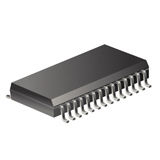
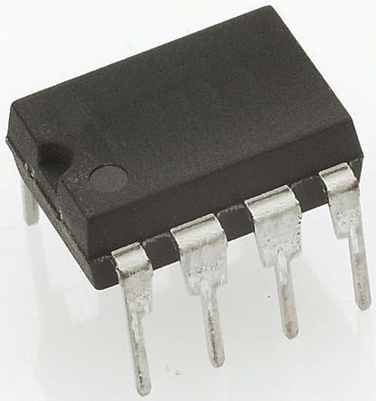
SN75LBC241DW
低功耗LinBiCMOS多个驱动器和接收器 LOW-POWER LinBiCMOS MULTIPLE DRIVERS AND RECEIVERS
The SN75LBC241 is a low-power LinBiCMOSTM line-interface device containing four independent drivers and five receivers. It is designed as a plug-in replacement for the Maxim MAX241. The SN75LBC241 provides a capacitive-charge-pump voltage generator to produce RS-232 voltage levels from a 5-V supply. The charge-pump oscillator frequency is 20 kHz. Each receiver converts RS-232 inputs to 5-V TTL/CMOS levels. The receivers have a typical threshold of 1.2 V and a typical hysteresis of 0.5 V and can accept ±30-V inputs. Each driver converts TTL/CMOS input levels into RS-232 levels.
The SN75LBC241 includes a receiver, a 3-state control line, and a low-power shutdown control line. When the EN\ line is high, receiver outputs are placed in the high-impedance state. When EN\ is low, normal operation is enabled.
The shutdown mode reduces power dissipation to less than 5 uW, typically. In this mode, receiver outputs have high impedance, driver outputs are turned off, and the charge-pump circuit is turned off. When SHUTDOWN is high, the shutdown mode is enabled. When SHUTDOWN is low, normal operation is enabled.
This device has been designed to conform to A/EIA-232-F and ITU Recommendation V.28.
The SN75LBC241 has been designed using LinBiCMOS technology and cells contained in the Texas Instruments LinASICTM library. Use of LinBiCMOS circuitry increases latch-up immunity in this device over an all-CMOS design.
The SN75LBC241 is characterized for operation from 0°C to 70°C. View datasheet View product folder

