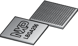
LPC1837JET256,551
LPC18 系列 180 MHz 1 MB 闪存 136 kB RAM 32位 微控制器 - LBGA-256
* Processor core * ARM Cortex-M3 processor, running at CPU frequencies of up to 180 MHz * ARM Cortex-M3 built-in Memory Protection Unit MPU supporting eight regions * ARM Cortex-M3 built-in Nested Vectored Interrupt Controller NVIC * Non-maskable Interrupt NMI input * JTAG and Serial Wire Debug, serial trace, eight breakpoints, and four watch points * Enhanced Trace Module ETM and Enhanced Trace Buffer ETB support * System tick timer * On-chip memory * Up to 1 MB on-chip dual bank flash memory with flash accelerator * 16 kB on-chip EEPROM data memory * 136 kB SRAM for code and data use * Multiple SRAM blocks with separate bus access * 64 kB ROM containing boot code and on-chip software drivers * 64 bit of One-Time Programmable OTP memory for general-purpose use * Clock generation unit * Crystal oscillator with an operating range of 1 MHz to 25 MHz * 12 MHz internal RC oscillator trimmed to 2 % accuracy over temperature andvoltage 1 % accuracy for Tamb = 0 °C to 85 °C * Ultra-low power RTC crystal oscillator * Three PLLs allow CPU operation up to the maximum CPU rate without the need fora high-frequency crystal. The second PLL can be used with the High-speed USB,the third PLL can be used as audio PLL * Clock output * Configurable digital peripherals * State Configurable Timer SCT subsystem on AHB * Global Input Multiplexer Array GIMA allows to cross-connect multiple inputs andoutputs to event driven peripherals like timers, SCT, and ADC0/1 * Serial interfaces * Quad SPI Flash Interface SPIFI with 1-, 2-, or 4-bit data at rates of up to52 MB per second * 10/100T Ethernet MAC with RMII and MII interfaces and DMA support for highthroughput at low CPU load. Support for IEEE 1588 time stamping/advanced timestamping IEEE 1588-2008 v2 * One High-speed USB 2.0 Host/Device/OTG interface with DMA support andon-chip high-speed PHY USB0 * One High-speed USB 2.0 Host/Device interface with DMA support, on-chipfull-speed PHY and ULPI interface to an external high-speed PHY USB1 * USB interface electrical test software included in ROM USB stack * Four 550 UARTs with DMA support: one UART with full modem interface; oneUART with IrDA interface; three USARTs support UART synchronous mode and asmart card interface conforming to ISO7816 specification * Up to two C_CAN 2.0B controllers with one channel each. Use of C_CAN controllerexcludes operation of all other peripherals connected to the same bus bridge * Two SSP controllers with FIFO and multi-protocol support. Both SSPs with DMAsupport * One Fast-mode Plus I²C-bus interface with monitor mode and with open-drain I/Opins conforming to the full I²C-bus specification. Supports data rates of up to1 Mbit/s * One standard I²C-bus interface with monitor mode and standard I/O pins * Two I²S interfaces with DMA support, each with one input and one output * Digital peripherals * External Memory Controller EMC supporting external SRAM, ROM, NOR flash,and SDRAM devices * LCD controller with DMA support and a programmable display resolution of up to1024H x 768V. Supports monochrome and color STN panels and TFT color panels;supports 1/2/4/8 bpp Color Look-Up Table CLUT and 16/24-bit direct pixelmapping * SD/MMC card interface * Eight-channel General-Purpose DMA controller can access all memories on theAHB and all DMA-capable AHB slaves * Up to 164 General-Purpose Input/Output GPIO pins with configurablepull-up/pull-down resistors * GPIO registers are located on the AHB for fast access. GPIO ports have DMAsupport * Up to eight GPIO pins can be selected from all GPIO pins as edge and levelsensitive interrupt sources