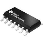
SN74LS628DR
压控振荡器 14-SOIC 0 to 70
These voltage-controlled oscillators VCOs are improved versions of the original VCO family: SN54LS124, SN54LS324 thru SN54LS327, SN74LS124, and SN74LS324 thru SN74LS327. These new devices feature improved voltage-to-frequency linearity, range, and compensation. With the exception of the "LS624 and "LS628, all of these devices feature two independent VCOs in a single monolithic chip. The "LS624, "LS625, "LS626, and "LS628 have complementary Z outputs. The output frequency for each VCO is established by a single external component either a capacitor or crystal in combination with voltage-sensitive inputs used for frequency control and frequency range. Each device has a voltage-sensitive input for frequency control; however, the "LS624, "LS628, and "LS629 devices also have one for frequency range. See Figures 1 thru 6.
The "LS628 offers more precise temperature compensation than its "LS624 counterpart. The "LS624 features a 600 ohm internal timing resistor. The "LS628 requires a timing resistor to be connected externally across Rext pins. Temperature compensation will be improved due to the temperature coefficient of the external resistor.
Figure 3 and Figure 6 contain the necessary information to choose the proper capacitor value to obtain the desired operating frequency.
A single 5-volt supply can be used: however, one set of supply voltage and ground pins VCC and GND is provided for the enable, synchronization-gating, and output sections, and a separate set OSC VCC and OSC GND is provided for the oscillator and associated frequency-control circuits so that effective isolation can be accomplished in the system. For operation of frequencies greater than 10 MHz, it is recommended that two independent supplies be used. Disabling either VCO of the "LS625 and "LS625 and "LS627 can be achieved by removing the appropriate OSC VCC. An enable input is provided on the "LS624, "LS626, "LS628, and "LS629. When the enable input is low, the output is enabled: when the enable input is high, the internal oscillator is disabled, Y is high, and Z is low. Caution! Crosstalk may occur in the dual devices "LS625, "LS626, "LS627 and "LS629 when both VCOs are operated simultaneously. To minimize crosstalk, either of the following are recommended: A If frequencies are widely separated, use a 10-μh inductor between VCC pins. B If frequencies are closely spaced, use two separate VCC supplies or place two series diodes between the VCC pins.
The pulse-synchronization-gating section ensures that the first output pulse is neither clipped nor extended. The duty cycle of the square-wave output is fixed at approximately 50 percent.
The SN54LS624 thru SN54LS629 are characterized for operation over the full military temperature range of -55°C to 125°C. The SN74LS624 thru SN74LS629 are characterized for operation from 0°C to 70°C.
View datasheet View product folder

