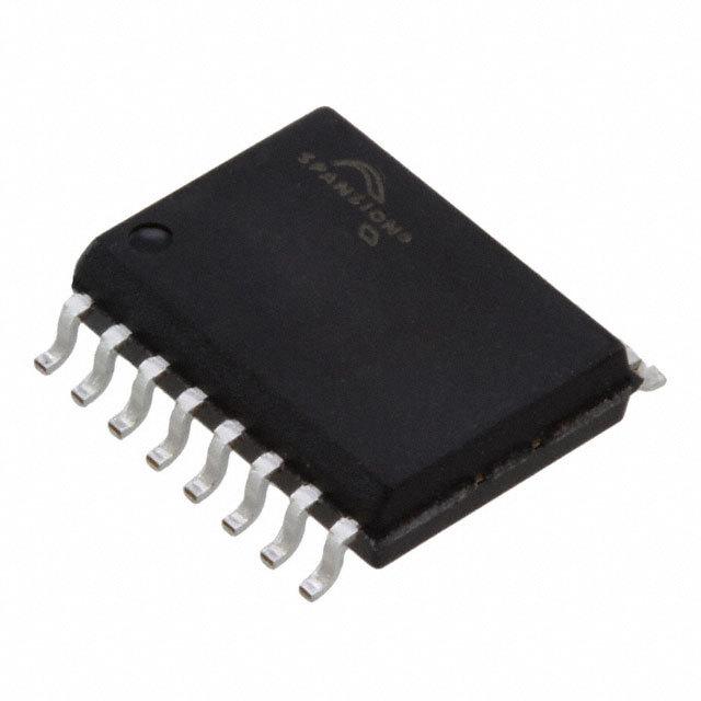
S25FL164K0XMFI011
SPANSION S25FL164K0XMFI011 闪存, 或非, 64 Mbit, 8M x 8位, 108 MHz, SPI, SOIC, 8 引脚
The is a non-volatile Flash Memory Device, connects to a host system via a serial peripheral interface SPI. Traditional SPI single bit serial input and output single I/O or SIO is supported as well as optional two bit Dual I/O or DIO and four bit Quad I/O or QIO serial protocols. This multiple width interface is called SPI Multi-I/O or MIO. The SIO protocol uses Serial Input SI and Serial Output SO for data transfer. The DIO protocols use IO0 and IO1 to input or output two bits of data in each clock cycle. The write protect WP# input signal option allows hardware control over data protection. Software controlled commands can also manage data protection.
- .
- SPI Clock Polarity and Phase Modes 0 and 3
- .
- Command Subset and Footprint Compatible with S25FL-K
- .
- Normal Read Serial, Fast Read Serial, Dual Read and Quad Read
- .
- Serial-input Page Program up to 256 Bytes
- .
- Program Suspend and Resume
- .
- Uniform Sector Erase 4kb
- .
- Uniform Block Erase 64kb
- .
- Chip Erase
- .
- Erase Suspend and Resume
- .
- 100K Program-erase Cycles on Any Sector, Minimum
- .
- 20-year Typical Data Retention
- .
- Three 256-byte Security Registers with OTP Protection
- .
- Low Supply Voltage Protection of Entire Memory
- .
- Pointer-based Security Protection Feature
- .
- Top/Bottom Relative Block Protection Range, 4kb to All of Memory
- .
- 8-byte Unique ID for Each Device
- .
- Non-volatile Status Register Bits Control Protection Modes
- .
- 90nm Floating Gate Technology
Exposure to absolute maximum ratings may affect device reliability, exposure beyond absolute maximum ratings may cause permanent damage.