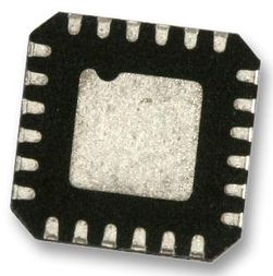
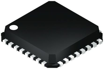
AD9576BCPZ
ANALOG DEVICES AD9576BCPZ ASYNC CLOCK GENERATOR, DUAL PLL, LFCSP64 New
Product Details
The AD9576 provides a multiple output clock generator function comprising two dedicated phase-locked loop PLL cores with flexible frequency translation capability, optimized to serve as a robust source of asynchronous clocks for an entire system, providing extended operating life within frequency tolerance through monitoring of and automatic switchover between redundant crystal XTAL inputs with minimized switching, induced transients. The fractional-N PLL design is based on the Analog Devices, Inc., proven portfolio of high performance, low jitter frequency synthesizers to maximize network performance, whereas the integer-N PLL provides general-purpose clocks for use as CPU and field-programmable gate array FPGA reference clocks.
The AD9576 uses pin strapping to select among a multitude of power-on ready configurations for its 11 output clocks, which require only the connection of external pull-up or pull-down resistors to the appropriate pin program reader pins PPRx. These pins provide control of the internal dividers for establishing the desired frequency translations, clock output functionality, and input reference functionality. These parameters can also be manually configured through a serial port interface SPI.
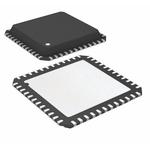
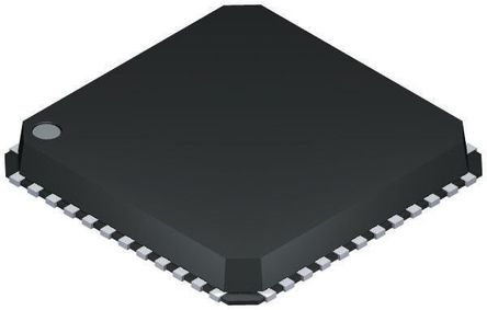
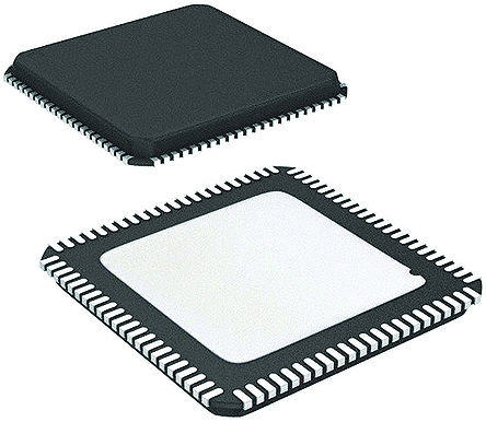
The AD9576 is packaged in a 64-lead, 9 mm × 9 mm LFCSP, requiring only a single 2.5 V or 3.3 V supply. The operating temperature range is −40°C to +85°C.
Each OUTx output is differential and contains two pins: OUTx and OUTx. For simplicity, the term OUTx refers to the functional output block containing these two pins..
Applications
- .
- Ethernet line cards, switches, and routers
- .
- Baseband units
- .
- SATA and PCI express
- .
- Low jitter, low phase noise clock generation
- .
- Asynchronous clock generation
### Features and Benefits
- .
- Single, low phase noise, fully integrated VCO/fractional-N PLL core
- .
- VCO range: 2375 MHz to 2725 MHz
- .
- Integrated loop filter requires a single external capacitor
- .
- 2 differential, XTAL, or single-ended reference inputs
- .
- Reference monitoring capability
- .
- Automatic redundant XTAL switchover
- .
- Minimal transient, smooth switching
- .
- Typical RMS jitter
- .
- <0.3 ps 12 kHz to 20 MHz, integer-N translations
- .
- <0.5 ps 12 kHz to 20 MHz, fractional-N translations
- .
- Input frequency
- .
- 8 kHz, 1.544 MHz, 2.048 MHz, and 10 MHz to 325 MHz
- .
- Preset frequency translations via pin strapping PPRx
- .
- Using a 25 MHz input reference
- .
- 24.576 MHz, 25 MHz, 33.33 MHz, 50 MHz, 70.656 MHz, 100 MHz, 125 MHz, 148.5 MHz, 156.25 MHz, 161.1328 MHz, 312.5 MHz, 322.2656 MHz, 625 MHz, or 644.5313 MHz
- .
- Using a 19.44 MHz input reference
- .
- 50 MHz, 100 MHz, 125 MHz, 156.25 MHz, 161.1328 MHz, or 644.5313 MHz
- .
- Using a 30.72 MHz input reference
- .
- 25 MHz, 50 MHz, 100 MHz, 125 MHz, or 156.25 MHz
- .
- Single, general-purpose, fully integrated VCO/integer-N PLL core
- .
- VCO range: 750 MHz to 825 MHz
- .
- Integrated loop filter
- .
- Independent, duplicate reference input or operation from the fractional-N PLL active reference input
- .
- Input frequency: 25 MHz
- .
- Preset frequency translations via pin strapping PPRx
- .
- 25 MHz, 33.33 MHz, 50 MHz, 66.67 MHz, 100 MHz, 133.33 MHz, 200 MHz, or 400 MHz
- .
- Up to 3 copies of reference clock output
- .
- 11 pairs of configurable differential outputs
- .
- Output drive formats
- .
- 3 outputs: HSTL, LVDS, HCSL, 1.8 V CMOS, 2.5 V/3.3 V CMOS
- .
- 8 outputs: HSTL, LVDS, or 1.8 V CMOS
- .
- 2.5 V or 3.3 V single-supply operation