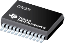
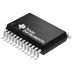
CDC351
具有三态输出的 1 线路至 10 线路 3.3V 时钟驱动器
The is a high-performance clock-driver circuit that distributes one input A to ten outputs Y with minimum skew for clock distribution. The output-enable OE\ input disables the outputs to a high-impedance state. The CDC351 operates at nominal 3.3-V VCC.
The propagation delays are adjusted at the factory using the P0 and P1 pins. The factory adjustments ensure that the part-to-part skew is minimized and is kept within a specified window. Pins P0 and P1 are not intended for customer use and should be connected to GND.
- .
- Low Output Skew, Low Pulse Skew for Clock-Distribution and Clock-Generation Applications
- .
- Operates at 3.3-V VCC
- .
- LVTTL-Compatible Inputs and Outputs
- .
- Supports Mixed-Mode Signal Operation 5-V Input and Output Voltages With 3.3-V VCC
- .
- Distributes One Clock Input to Ten Outputs
- .
- Distributed VCC and Ground Pins Reduce Switching Noise
- .
- High-Drive Outputs -32-mA IOH, 32-mA IOL
- .
- State-of-the-Art EPIC-IIBTM BiCMOS Design Significantly Reduces Power Dissipation
- .
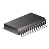
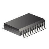
- Package Options Include Plastic Small-Outline DW and Shrink Small-Outline DB Packages
EPIC-IIB is a trademark of Texas Instruments Incorporated.