CD4042BE
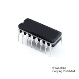
TEXAS INSTRUMENTS CD4042BE 逻辑芯片, 时钟D型锁存器, 4路, 16DIP
The is a CMOS Quad-clocked "D" Latch, each strobed by a common clock. Complementary buffered outputs are available from each circuit. The impedance of the n and p-channel output devices is balanced and all outputs are electrically identical. Information present at the data input is transferred to outputs Q and Q\ during the CLOCK level which is programmed by the POLARITY input. For POLARITY=0 the transfer occurs during the 0 CLOCK level and for POLARITY=1 the transfer occurs during the 1 CLOCK level. The outputs follow the data input providing the CLOCK and POLARITY levels defined above are present. When a CLOCK transition occurs positive for POLARITY=0 and negative for POLARITY=1 the information present at the input during the CLOCK transition is retained at the output until an opposite CLOCK transition occurs.
- .
- Clock polarity control
- .
- Q and Q\ outputs
- .
- Common clock
- .
- Low power TTL compatible
- .
- Standardized, symmetrical output characteristics
- .
- 100% Tested for quiescent current at 20V


