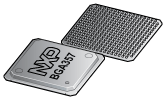
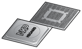
MPC866PCZP100A
MPU PowerQUICC MPC8xx Processor RISC 32Bit 0.18um 100MHz 3.3V 357Pin BGA Tray
Overview
MPC866 PowerQUICC™ Family is a 0.18 micron version of the MPC862 PowerQUICC® Family and can operate up to 133 MHz on the MPC8xx core with a 66 MHz external bus. The MPC866 Family has a 1.8 V core and has a 3.3 V I/O operation with 5 V TTL compatibilty. The MPC866 Integrated Communications Controller Family is a versatile one-chip integrated microprocessor and peripheral combination that can be used in a variety of controller applications. It particularly excels in both communications and networking systems.
The MPC866 Family is a a Power Architecture-based derivative of Our Quad Integrated Communications Controller PowerQUICC. The CPU on the MPC866 is the MPC8xx core, a 32-bit microprocessor built on Power Architecture technology, incorporating memory management units MMUs and instruction and data caches. The MPC866P is the superset of this family of devices.
MoreLess
## Features
Embedded MPC8xx core up to 133 MHz
* Maximum frequency operation of the external bus is 66 MHz
* Single-issue, 32-bit core compatible with Power Architecture technology with 32, 32-bit general-purpose registers GPRs
* The MPC866 Family provides enhanced ATM functionality as found on the MPC862. The MPC866 adds major new features available in "enhanced SAR" ESAR mode, including the following:
* Improved operation, administration and maintenance OAM support
* OAM performance monitoring PM support
* Multiple APC priority levels available to support a range of traffic pace requirements
* Port-to-port switching capability without the need for RAM-based microcode
* Simultaneous MII 100Base-T and UTOPIA half-duplex capability
* Optional statistical cell counters per PHY
* UTOPIA level 2 compliant interface with added FIFO buffering to reduce the total cell transmission time. The earlier UTOPIA level 1 specification is also supported.
* Parameter RAM for both SPI and I2C can be relocated without RAM-based microcode
* Supports full-duplex UTOPIA both master ATM side and slave PHY side operation using a "split" bus
* AAL2/VBR functionality is ROM-resident
* Up to 32-bit data bus dynamic bus sizing for 8, 16, and 32 bits
* 32 address lines
* Memory controller eight banks
* General-purpose timers
* Fast Ethernet controller FEC
* System integration unit SIU
* Interrupts
* Communications processor module CPM
* Four baud rate generators
* Four SCCs serial communication controllers
* Two SMCs serial management channels
* One SPI serial peripheral interface
* One I2C inter-integrated circuit port
* Time-slot assigner TSA
* Parallel interface port PIP
* PCMCIA interface
* Debug interface
* 1.8 V Core and 3.3 V I/O operation with 5-V TTL compatibility
* 357-pin ball grid array BGA package
## Features Comparison Table
### MPC866 Family Versions and Masks
| Qual | Process | Mask | IMMR [16:31]
\---|---|---|---|---
**Rev 0.3** | MC | HiP6W | 3L90H | 0x0800
**Rev A.0** | MC | HiP6W | 0L96R | 0x0801
Note 1: Where nn = 50, 66, 100, or 133