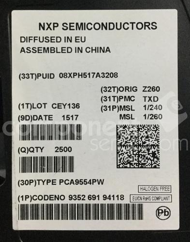
PCA9515ADP/G,118
I2C-bus repeater
Overview
The PCA9515A is a CMOS integrated circuit intended for application in I²C-bus and SMBus systems.
While retaining all the operating modes and features of the I²C-bus system, it permits extension of the I²C-bus by buffering both the data SDA and the clock SCL lines, thus enabling two buses of 400 pF.
The I²C-bus capacitance limit of 400 pF restricts the number of devices and bus length. Using the PCA9515A enables the system designer to isolate two halves of a bus, thus more devices or longer length can be accommodated. It can also be used to run two buses, one at 5 V and the other at 3.3 V or a 400 kHz and 100 kHz bus, where the 100 kHz bus is isolated when 400 kHz operation of the other is required.
** **Two or more** PCA9515A**s cannot be put in series** **. The PCA9515A design does not allow this configuration. Since there is no direction pin, slightly different "legal" low voltage levels are used to avoid lock-up conditions between the input and the output. A "regular LOW" applied at the input of a PCA9515A will be propagated as a "buffered LOW" with a slightly higher value. When this "buffered LOW" is applied to another PCA9515A, PCA9516A or PCA9518/A in series, the second PCA9515A, PCA9516A or PCA9518/A will not recognize it as a "regular LOW" and will not propagate it as a "buffered LOW" again. The PCA9510/A, PCA9511/A, PCA9512/A, PCA9513/A, PCA9514/A cannot be used in series with the PCA9515A, PCA9516A or PCA9518/A, but can be used in series with themselves since they use shifting instead of static offsets to avoid lock-up conditions.
The output pull-down of each internal buffer is set for approximately 0.5 V, while the input threshold of each internal buffer is set about 0.07 V lower, when the output is internally driven LOW. This prevents a lock-up condition from occurring.
MoreLess
## Features
* 2-channel, bidirectional buffer
* I²C-bus and SMBus compatible
* Active HIGH repeater enable input
* Open-drain input/outputs
* Lock-up free operation
* Supports arbitration and clock stretching across the repeater
* Accommodates Standard-mode and Fast-mode I²C-bus devices and multiple masters
* Powered-off high-impedance I²C-bus pins
* Operating supply voltage range of 2.3 V to 3.6 V
* 5.5 V tolerant I²C-bus and enable pins
* 0 Hz to 400 kHz clock frequency the maximum system operating frequency may be less than 400 kHz because of the delays added by the repeater
* ESD protection exceeds 2000 V HBM per JESD22-A114 and 1000 V CDM per JESD22-C101
* Latch-up testing is done to JEDEC Standard JESD78 which exceeds 100 mA
* Packages offered: SO8, TSSOP8 MSOP8, HWSON8
## Features