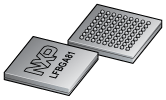
PX1011B-EL1/G,551
Telecommunications, NXP### 以太网通信一系列以太网通信控制器、收发器和交换 IC
Overview
The PX1011B is a high-performance, low-power, single-lane PCI Express electrical PHYsical layer PHY that handles the low level PCI Express protocol and signaling. The PX1011B PCI Express PHY is compliant to the PCI Express Base Specification, Rev. 1.0a, and Rev. 1.1. The PX1011B includes features such as Clock and Data Recovery CDR, data serialization and de-serialization, 8b/10b encoding, analog buffers, elastic buffer and receiver detection, and provides superior performance to the Media Access Control MAC layer devices.
The PX1011B is a 2.5 Gbit/s PCI Express PHY with 8-bit data PXPIPE interface. Its PXPIPE interface is a superset of the PHY Interface for the PCI Express PIPE specification, enhanced and adapted for off-chip applications with the introduction of a source synchronous clock for transmit and receive data. The 8-bit data interface operates at 250 MHz with SSTL_2 signaling. The SSTL_2 signaling is compatible with the I/O interfaces available in FPGA products.
The PX1011B PCI Express PHY supports advanced power management functions. The PX1011BI is for the industrial temperature range -40 ℃ to +85 ℃. Automotive AEC-Q100 compliant version PX1011B-EL1/Q900 is available.
MoreLess
## Features
**2.1 PCI Express interface**
* Compliant to PCI Express Base Specification 1.1
* Single PCI Express 2.5 Gbit/s lane
* Data and clock recovery from serial stream
* Serializer and De-serializer SerDes
* Receiver detection
* 8b/10b coding and decoding, elastic buffer and word alignment
* Supports loopback
* Supports direct disparity control for use in transmitting compliance pattern
* Supports lane polarity inversion
* Low jitter and Bit Error Rate BER
**2.2 PHY/MAC interface**
* Based on Intel PHY Interface for PCI Express architecture v1.0 PIPE
* Adapted for off-chip with additional synchronous clock signals PXPIPE
* 8-bit parallel data interface for transmit and receive at 250 MHz
* 2.5 V SSTL_2 class I signaling
**2.3 JTAG interface**
* JTAG IEEE 1149.1 boundary scan interface
* Built-In Self Test BIST controller tests SerDes and I/O blocks at speed
* 3.3 V CMOS signaling
**2.4 Power management**
* Dissipates < 300 mW in L0 normal mode
* Support power management of L0, L0s and L1
**2.5 Clock**
* 100 MHz external reference clock with ±300 ppm tolerance
* Supports spread spectrum clock to reduce EMI
* On-chip reference clock termination
**2.6 Miscellaneous**
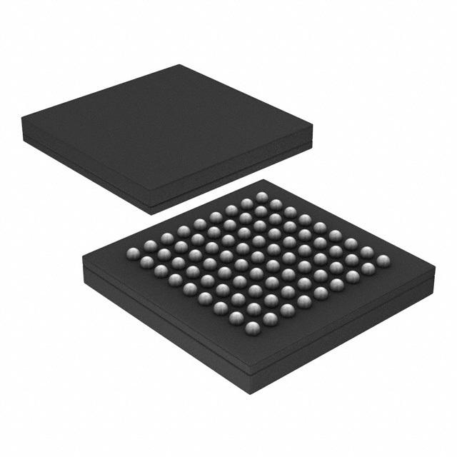
* LFBGA81 leaded or lead-free packages
* Operating ambient temperature
* Commercial: 0 ℃ to +70 ℃
* Industrial: -40 ℃ to +85 ℃
* ESD protection voltage for Human Body Model HBM: 2000 V
## Features